 Christoph
Why do you have 0201 or similarly sized components on your PCB? Probably to save space, or because of some more occult reasons like stray capacitance or whatnot.
Courtyards
Courtyards create sufficient space between components to ensure somewhat minimal insulation, allow for placement errors, support the reflow process and provide some extra space where the pick and place machine can maneuver. All those make sense. However, we usually encounter large, rectangular courtyards - and that leaves room for improvement. Most of the time we don't need them to achieve any of the above, because most components are rather flat (reflow, maneuvering), the signals require only little insulation and the pnp machine will be able do its job just fine even when the layout is very dense.
So to allow for denser layouts we can hide the courtyard layer and ignore courtyard violations (or configure them to be warnings or just messages), or redesign the courtyards. Both make sense:
- switch them off to get no warnings at all
- redesign them for components whose footprint doesn't make it absolutely clear where the physical part ends (if it's placed correctly)
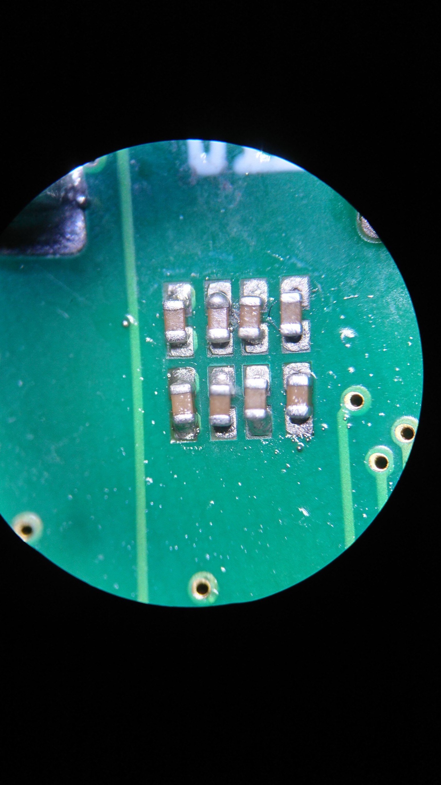
Example: 0603 capacitors, KiCad stock footprint, with and without courtyards. The caps to the right are moved as close to each other as the design rules (0.1 mm / 0.1 mm) allow.
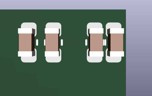
With good tweezers that's no problem. 0402 and 0201 are similar, because the design rules stay the same so there's always a minimum gap between the components.
One more thing to note about this style of passives: If their pads don't overlap with other parts, you cannot have a physical collision between parts and the design rule check will make sure that you don't have these overlaps. The pads are larger than the actual package.
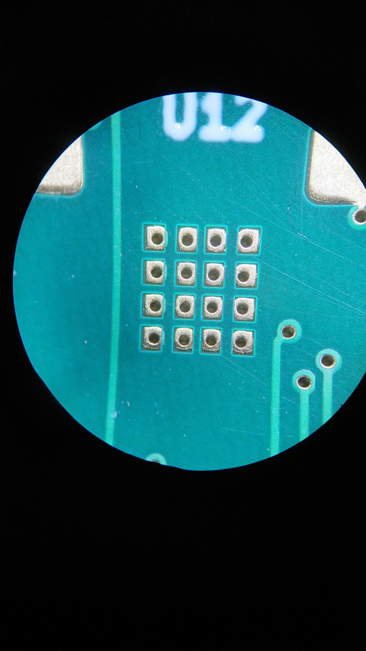
Example: QFN with non-rectangular courtyard. QFNs have corners that occupy extend between the pad rows:
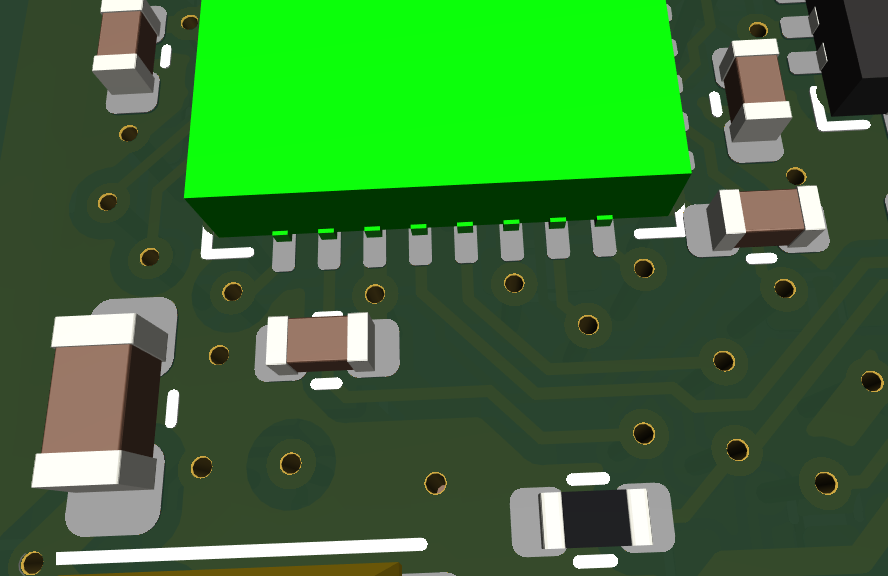
Also, if your EDA software has a 3D preview, make sure your 3D models are sufficiently accurate. Then the 3D view can tell you if it really fits even if you violate the courtyards:
Some even say that courtyards are luxury. I wouldn't go that far, but using stock rectangular courtyards feels a bit excessive.
Vias in pads vs. via-in-pad
Vias occupy space if they're placed outside of pads. And quite often we're tempted to place them inside pads, which is absolutely fine when the PCB is made with proper via-in-pad tech. When we now head over to, say, electronics stack exchange, we'll quickly realize that placing an "open" via in a pad will quickly result in great-great-grandma raising from her grave to grab us by the ear and pull us to the table because it's time for dinner before we can even release the mouse button. And for a production board that would probably be correct. But we're building a prototype and proper via-in-pad is expensive.
So - again - what can we get away with? Turns out, A LOT. Here's a bunch of 0201 caps on 0402 footprints with open vias in pads:
Honestly that still needed a little touchup and cleaning, but it works!
So if it's really an advantage for your layout: just do it. A via in an 1206 pad is certainly not a problem at all, and even down to 0603 it's not really a problem. Below that, you'll want to fill the via with solder first. Then it's business as usual. Vias in pads are ok.
Prepare for double sided assembly
The other side is valuable area for components. It's a little trickier to assemble, of course. One thing I try to do is to put all components that require high-temp solder on the same same side. These are
- Anything with increased mechanical stress (connectors, switches, buzzers, ...)
- BGAs where we can't choose the solder alloy ourselves
Another thing you can try to do is to design the PCB such that one side has only very flat parts.
But both of these points are optional, so don't worry about it too much.
Discussions
Become a Hackaday.io Member
Create an account to leave a comment. Already have an account? Log In.