 BleakyTex
Towards efficient boost converter architecture
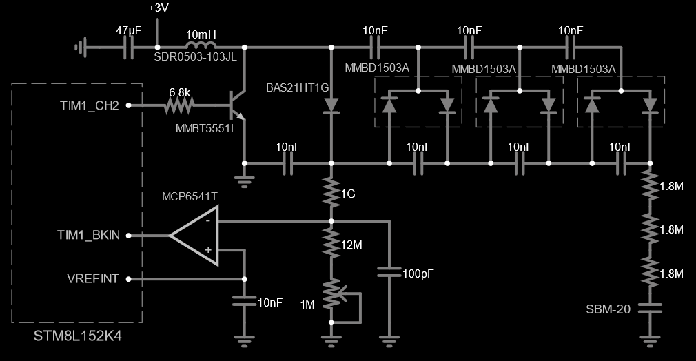
Most DIY Geiger counters that I've seen on the Internet have very simple architecture: just an oscillator driving a transistor, sometimes with Zener diodes to limit the output voltage. This approach is inefficient, so I've decided to make a boost converter that's both efficient and compact. The first thing that comes to mind is that the converter has to disable the oscillator when it's not needed. This approach is described in an appnote by Maxim Integrated:
Here they're using a comparator to control the oscillator output: when the feedback voltage is less than the reference voltage the oscillator is enabled, and vice versa. Since a Geiger tube only consumes energy when hit by a particle, the oscillator shall remain idle most of the time, and that saves a lot of power. Also there's a 6-stage voltage multiplier, so we can feed the lower output voltage from its first stage to a feedback divider, thus minimizing the current through it. I'll be reducing losses in the feedback divider as much as possible since it consumes the most power in the circuit above.
Setting up the microcontroller
One huge benefit of microcontrollers is that they have peripherals that can replace discrete components, saving power and PCB space. In our case we can use a microcontroller to replace a voltage reference and an oscillator in the circuit above (and even a comparator if we wouldn't have to drive a 4-backplane LCD).
We should set the MCU to output a reference voltage and a comparator-controlled PWM: when the comparator output is LOW (voltage divider voltage less than reference voltage), the timer generates PWM, otherwise it sets its output to LOW, closing the transistor. The only timer that we can use is TIM1 because pins, tied to other timers are needed for other functions. This timer has a break input which disables timer's output when it receives a signal, which is exactly what we need. The schematic is as follows:
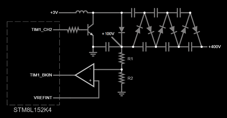
To use a lower value inductor for better energy and space efficiency, we'll set the PWM generation for shortest positive pulse possible, i.e. highest frequency and lowest duty cycle; the best we can get with a timer is half the system clock. The MCU is clocked from 32.768 kHz crystal, which means 50% duty cycle PWM at 16.384 kHz.
To write the code I'll be using the IAR Embedded Workbench for STM8.
#include "iostm8l152k4.h"

void Clock_Init(void)
{
  CLK_SWCR_bit.SWEN = 1;         // Prepare to change the clock source
  CLK_SWR = 0x08;                // Change the clock source to LSE
  while(CLK_SWCR_bit.SWBSY==1);  // Wait until it starts up
  CLK_CKDIVR = 0x00;             // Change the clock prescaler from default /8 to /1
  CLK_ICKCR_bit.HSION = 0;
  CLK_ICKCR_bit.LSION = 0;       // Disable internal oscillators
}

void VREF_Init(void)
{
  while(!PWR_CSR2_bit.VREFINTF); // Wait for voltage reference to stabilize

  CLK_PCKENR2_bit.PCKEN25 = 1; // Enable clock for COMP peripheral
  COMP_CSR5_bit.VREFTRIG  = 2; // Disable Schmitt trigger on PD7 to reduce leakage
  COMP_CSR3_bit.VREFOUTEN = 1; // Enable VREF output
  RI_IOSR2_bit.CH8E = 1;       // Connect VREFOUT to PD7
  CLK_PCKENR2_bit.PCKEN25 = 0; // Disable clock for COMP, was only needed for init
}

void TIM_Init(void)
{
  /* TIM1 SETUP (SYSCLK/2 GATED BY EXTERNAL SIGNAL) */
  PD_DDR_bit.DDR4 = 1;         // Set PD4 to output mode
  PD_CR1_bit.C14 = 1;          // Set PD4 output to push-pull mode
  CLK_PCKENR2_bit.PCKEN21 = 1; // Enable TIM1 clock

  TIM1_ARRH = 0;
  TIM1_ARRL = 1;        // Highest frequency (16.384 kHz)
  TIM1_CCR2H = 0;
  TIM1_CCR2L = 1;       // Lowest duty cycle (50%)

  TIM1_BKR_bit.BKE = 1;      // Enable output break
  TIM1_CCMR2_bit.OC2M = 0x6; // Set output mode: PWM mode 1
  TIM1_CR1_bit.CEN = 1;      // Enable timer counter
  TIM1_CCER1_bit.CC2E = 1;   // Enable TIM1_CH2 output
  TIM1_BKR_bit.AOE = 1;      // Automatically recover from output break
}

int main(void)
{
  Clock_Init();
  VREF_Init();
  TIM_Init();
}
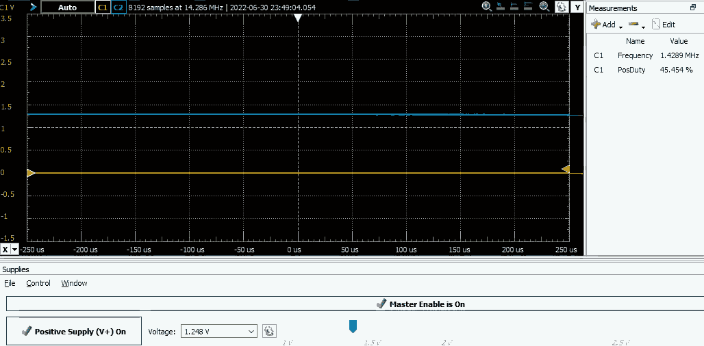
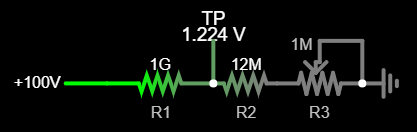
The beauty of this approach is that it's completely core independent — notice that that there is no code after initialization, the CPU isn't necessary to control the boost converter. Let's test if this works. I've connected a voltage source to the comparator's inverting terminal and the MCU should output PWM when the voltage is below reference (1.224V) and output LOW level otherwise:
Seems to work fine, let's move to the analog part of the boost converter.
Selecting components
Feedback resistors and voltage multiplication
As I've said, the feedback network (R1 and R2 on the circuit above) can easily be the biggest energy consumer in the whole circuit, so we should use resistors of the highest value and have the lowest feedback voltage possible. Feedback voltage depends on the number of multiplication stages. Initially I've built a booster with x12 multiplier but it had a parasitic oscillation issue which I failed to resolve.
I ended up with the x4 multiplier (as shown on the circuit above) which is compact and has reasonably low current consumption. We have to supply 400V to an SBM-20 tube, so the feedback voltage at the first multiplication stage shall be 400V / 4 = 100V. At this input voltage, the feedback divider output voltage should be equal to VREF — 1.224V.
I've got my hands on some 1GΩ resistors, so I'll use them for R1. Then R2 = 12.4MΩ. Resistors of this value are not available, so I've split it into a 12MΩ resistor and 1MΩ potentiometer, which will also allow to compensate for R1 and VREF tolerances:
Using a 100V for output feedback may seem horribly inefficient but let's calculate how much battery current the boost converter shall actually consume to drive the feedback network. For this we should write equations for the power consumed on both sides of the converter (low voltage side and high voltage side):
From this we can derive the battery current, consumed by the booster's feedback loop:
Of course, the real-world value will be higher because the efficiency of the boost converter is less than 100%. Also at lower battery voltages the current consumption will increase: 5.5µA at 1.8V (lowest operating voltage for the MCU). Still, I consider this acceptable, given that the total consumption of the device is 44µA at full battery and normal background radiation level.
Comparator
Since we are using very high value resistors, we should mind the load we put on the feedback voltage divider — the comparator must have a low input bias current (and a low quiescent current if we want long battery life). I'm using an MCP6541 comparator in this project because due to the chipageddon it was the only one available to me that met the requirements: 1pA input bias current, 600nA quiescent current. 3.3mV hysteresis is barely enough to provide enough noise immunity though, this is most likely the main reason I was unable to make a 12-stage voltage multiplier work. If I could, I'd use something like TLV7031 or TLV4051R1.
Inductor
Inductor selection directly influences the efficiency and maximum output power of the converter. I've chose SDR0503-103JL — 10mH inductor with 110Ω max series resistance because it was the highest value inductor available with reasonably small dimensions (I couldn't have an inductor with >3mm height). We want high inductance because of very low PWM frequency, and also high inductance reduces peak inductor current during converter operation which helps to reduce losses in a transistor, — high-voltage transistors don't handle high currents very well.
Let's see how much power our boost converter can provide with this inductor. To find it, we should find its peak current first. Current vs time formula for an inductor with series resistance is as follows:
where:
- VL — voltage applied to the inductor
- Ra — sum of resistances in inductor's current path: inductor series resistance, power supply ESR, transistor etc. For simplicity, I'll assume all resistances except inductor's negligible.
- L — inductance
To find the amount of energy, transferred during one PWM cycle, we should first find the current that the inductor builds up during transistor ON time (which will be its peak current). Our MCU outputs 16.384 kHz PWM with 50% duty cycle. Then:
where D — duty cycle. From this, the peak inductor current will be:
Here we're finding the peak current at the lowest supply voltage (1.8V) to find the worst case power output.
The energy, transferred during each PWM cycle is:
These energy transfers occur at 16.384 kHz rate, so maximum output power will be:
Now we will check if that's enough to drive the feedback divider and a Geiger tube. Feedback divider consumes:
With a Geiger tube things are more complicated. Given a fixed supply voltage, a Geiger tube consumes a fixed amount of charge during each registered event, however for some reason the amount of charge is not specified in datasheets. Fortunately, there is a rule of thumb: the tube consumes a charge, roughly equal to 1/3 of the total charge, held by tube's capacitance:
The maximum counting rate for an SBM-20 tube is 1400 CPS (Hz), so maximum consumed power will be:
So the total power, consumed by high-voltage part will be:
As you can see, we have plenty of headroom even with fully discharged battery.
Now let's talk about efficiency. The series resistance of our inductor is 110Ω, this obviously will significantly reduce efficiency. A simple way to check the efficiency (and estimate optimal tON) for given inductor is to compare the iL(t) graphs for lossless and lossy inductor. A formula for ideal inductor stems from the basic inductor equation:
I'll plot the inductor currents from t = 0 to tON.
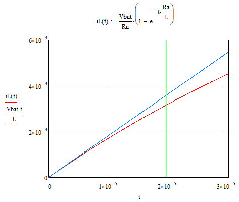
As we can see, as time increases, the graph of current in real inductor rises slower and slower, and eventually it will become a flat line because current will be limited by inductor's series resistance. Obviously, the more these graphs deviate from each other, the lower the efficiency will be. In our case, at t = tON, iL(real) / iL(ideal) = 0.85 (85%), so we're losing about 15% efficiency with this inductor. I think, this is acceptable, considering the small size of the inductor.
Transistor and its base resistor
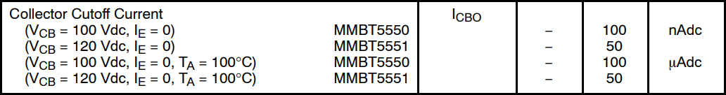
I was unable to find any suitable MOSFETs, so I resorted to bipolar transistors. And there's still not many to choose from: BCX41, BSR19A and MMBT5551 are the only ones I would use. I was able buy only the MMBT5551. There are two transistor parameters that I consider most important — collector leakage and collector-emitter saturation voltage at given collector and base currents.
Low leakage helps to reduce energy losses in the inductor, improving efficiency. The general idea to get low leakage is to have a big headroom in voltage rating . This transistor is rated for 160V, so we have 60V headroom.
Collector-emitter saturation voltage (VCEsat) is what causes energy losses in the transistor when it's open, so we want it to be as low as possible.
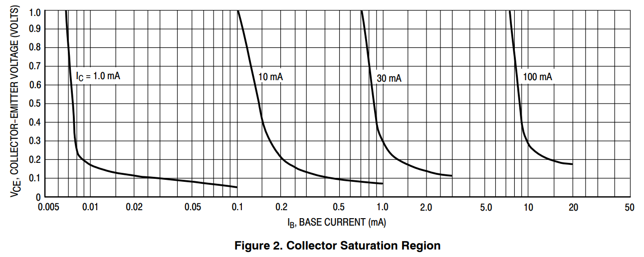
As you can see, VCEsat decreases as base current increases, so we should find a compromise between base current and VCEsat. The maximum collector current is equal to peak inductor current when the battery is at full capacity:
so we should use the second left graph to find the optimal base current Ib. The goal is to find Ib such that the sum of energy, lost on driving the base and energy, lost due to VCEsat, is minimal.
Energy, dissipated in every PWM cycle due to VCEsat:
This formula stems from definition of energy: E = P ⋅ t = VI ⋅ t. After integrating we get:
At this point we should take into account that the transistor will reduce the inductor voltage by VCEsat, which is reflected in formulas above.
Energy, dissipated in every PWM cycle to drive the transistor base is:
Here 0.7V is base-emitter voltage drop.
Now I'll just try various points on the graph and find the point with smallest Evce + Eb, which happens to be at Ib = 0.4 mA (with VCEsat = 0.1V and total loss being 35.3 nJ per cycle). Since we took this value from the graph for Ic = 10mA, we get:
And then the base resistor will be:
Closest value from E24 series is 7.5kΩ but 6.8kΩ from E12 series will work fine as well.
Tube anode resistors
The datasheet for SBM-20 tube recommends a 5.1MΩ anode resistor. Since we're optimizing the PCB size, we have to use small components. In our case we can use three SMD 0805 resistors in series: most of them are rated for 150V, so three of them should withstand 450V (given they have same value). If we use 1.8MΩ resistors, we'll get 5.4MΩ. which is close enough. At the last moment I realized I only have 2.2MΩ resistors, so I've used those and they work fine.
Diodes and capacitors for voltage multiplier
We are interested in three things here: appropriate voltage rating, low leakage and small footprint. In our case, components in voltage multiplier must be rated at least for the feedback voltage: 100V. Not double that, like most articles about voltage multipliers tell. In our case, the input voltage swings from 0V to 100V, not from -100V to 100V like these articles assume.
There are plenty of suitable diodes and capacitors, I've chose BAS21 and MMBD1503A diodes because they have small footprint and 10nF / 500V, SMD 0805 capacitors to have a reasonable voltage headroom to avoid capacitance derating. Some of you might ask if 10nF capacitors are enough to provide sufficient power for a Geiger tube. The equivalent output resistance of a voltage multiplier given all its capacitors are the same value is:
where n — number of multiplication stages. Obviously, this is more than enough to drive a 5.4MΩ anode resistor.
Testing and debugging
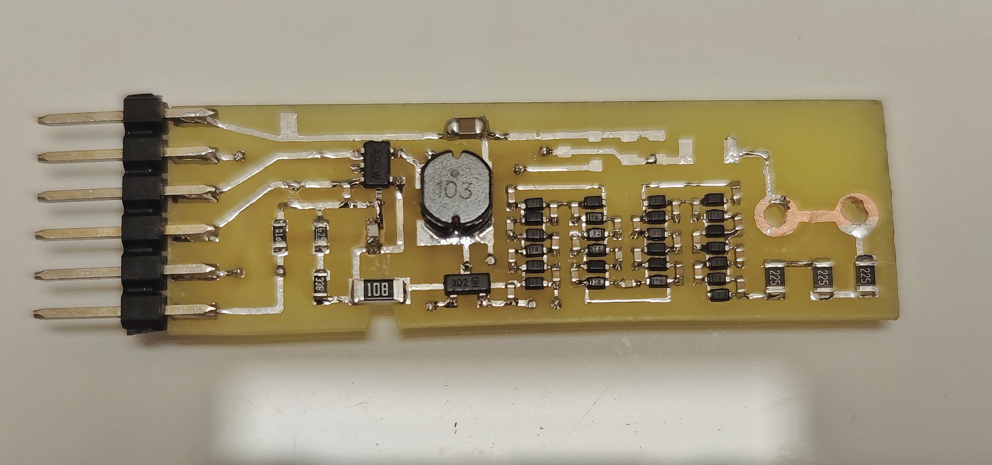
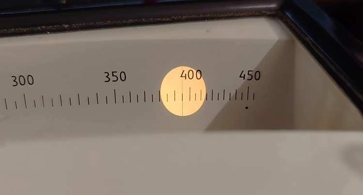
I've made a crude prototype to test the operation of my boost converter. I forgot to make proper photos, so here's one without voltage multiplier, — I was testing if the boost converter correctly outputs 100V, and it does. I was using STM8L-DISCOVERY board for software prototyping.
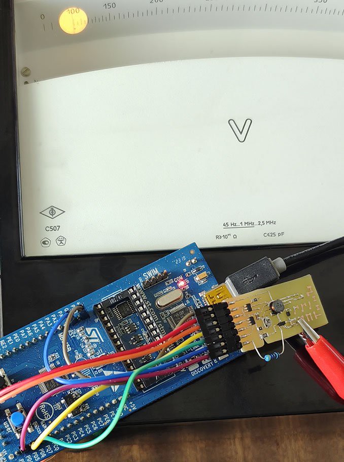
Notice that I am using an electrostatic voltmeter to measure the voltage because a regular multimeter will overload the boost converter and thus show a voltage, lower than the converter would output without multimeter leads connected. This voltmeter has 100GΩ input resistance, so it doesn't affect the operation of the boost converter. Also notice a small cutout on the bottom left of the PCB. I made it to reduce PCB leakage under the 1GΩ resistor which may reduce its effective resistance.
While the converter has correct output voltage, there was a problem — it was consuming a whopping 110µA current. I hooked the oscilloscope to the PWM output and comparator output and saw this:
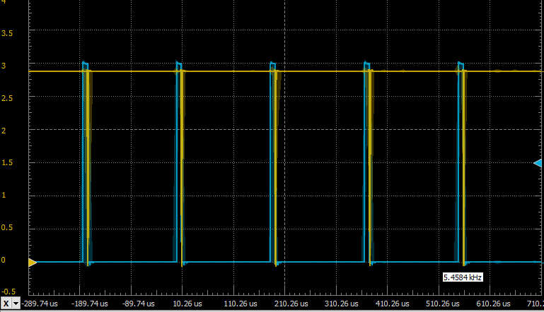
This looks nothing like a 16.384 kHz PWM with 50% duty cycle that we expect the MCU to generate, and it acts like this because the comparator sends very short breaking pulses to the MCU, which in turn makes PWM pulses much shorter than intended. Because of that, to maintain voltage, the MCU has to generate PWM almost non-stop because with such short positive pulses the converter cannot push too much power, and to make matters worse, the transistor doesn't even have time to fully open. Also fun fact, the oscillation occurs at 5.458 kHz which is exactly 3 times lower than 16.384 kHz. Go figure why that is.
Then I looked at VREF and saw this:
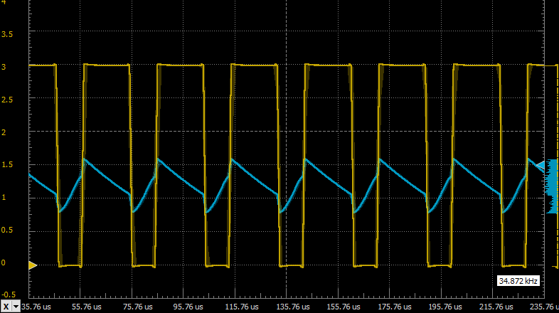
This is getting more and more weird. How can a comparator with 1pA input bias current load the VREF output so much that it causes 0.75V ripple on it?! I've tried replacing the comparator, to no avail. Guess I just got a bad batch of these comparators. Also apparently the oscilloscope loaded VREF output more than it could handle (it can't output more than 1 µA) and this shifted the oscillation frequency.
First thing that came to mind — bypass the VREF with a 10nF capacitor. This indeed reduced VREF ripple to ±1 mV (which I think is a lot for such a large capacitor and light load) but did not solve the oscillation problem at all. Then I assumed that the same thing happens on the feedback side and decided to bypass the feedback divider output as well. I couldn't just use whatever capacitor I wanted there because as capacitance increases, the leakage current increases as well and since we have a 1GΩ resistor in the feedback divider, at some point the leakage current of a bypass capacitor may become significant. So I've started with a small value — 10pF and started increasing it until the parasitic oscillation was gone, at 100pF. A healthy boost converter drives a transistor like this:
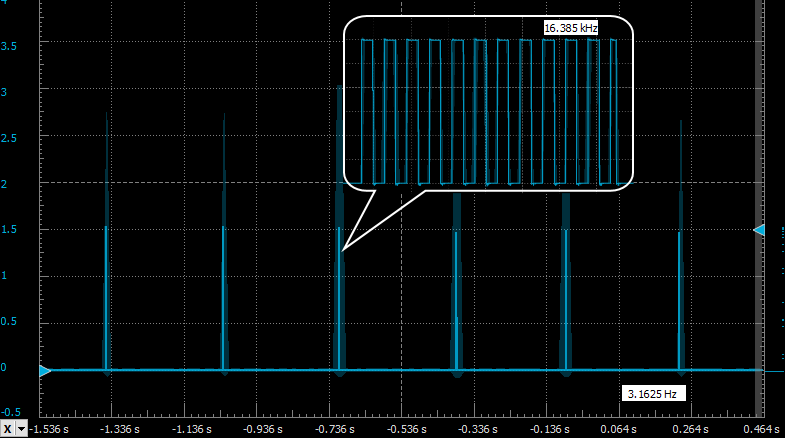
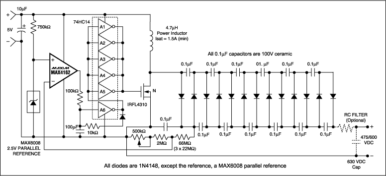
Now the converter consumes 7µA when idle (MCU consumption not included, just inductor+comparator) and I'm happy with this number. The final schematic is as follows:
And, of course, the final test — for the output voltage after multiplication.
Discussions
Become a Hackaday.io Member
Create an account to leave a comment. Already have an account? Log In.