 ElectroBoy
A single cell power bank is the most important/saver device in a small form factor when the charged devices are about to die. It can charge the battery-operated device like a power bank and the capacity depend on the battery cell you are using. The coolest thing is you can replace the battery or carry more than one charged battery.
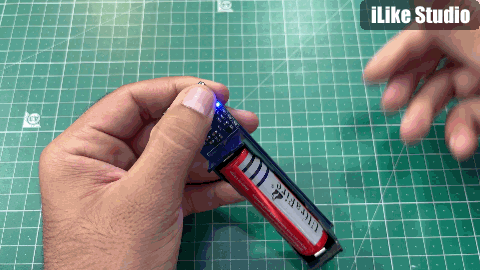
It acts same as power bank and having all the safety features like overvoltage/current protection and battery protection at under voltage. Now the battery percentage can also be monitored via embedded led lights. The circuit is operatable only at 3.7v, it can charge the single cell battery with MOSFET protection. Comes with a tactile switch used to power off/on the integrated circuit.
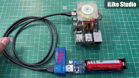
Additionally, a C-type charging port and USB type A power output with 5volts 1Ampere (Max) capacity. You can add a battery from 200MAH to 10,000MAH with the same circuit. Also have a charging coil upgradeable options to go with more than 3amp. I used JLCPCB SMT assembly service to complete my project, I selected only some components because these are not available to me and JLCPCB only charged $8 for the SMT assembly and a total of $30. Which includes the component cost + soldering cost + assembly + Shipping + PCB prototype and extra services. Get Quote now only on JLCPCB for SMT assembly orders.
Choosing the latest components:
The market is full of integrated circuit and the latest one offers better charging, discharging. Has better controlled output with minimum external components. Here we are using a power bank ic 5306 which is designed to handle all these conditions and has a lot of features. See datasheet from here. In the single IC you will get on chip charging protection and battery boosting.
Components Required:
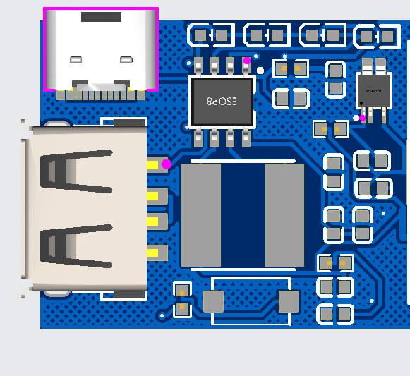
- IP 5306 ic
- 1.5uH inductor coil
- Tactile button
- 22uf, 10uf, 1uf and 100nf ceramic capacitors
- 10k, 1k resistor
- 0603 Led light
- USB type C and A
- Battery holder
- Custom PCB from JLCPCB
Circuit diagram:
The circuit has 4 led indictors for the battery percentage, this IP 5306 is dedicatedly designed for power bank applications. Because this has single battery charging (pair more in parallel), protection and boosted 5volt output capabilities. The tactile button is a very great feature which helps to turn on/off the device manually.
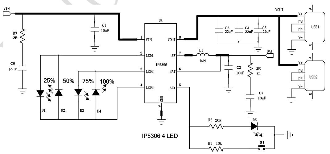
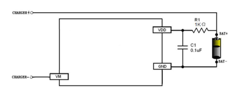
The filtered output can be archived by using high quality coils and capacitors. Which defines the total quality factor of any product. I also added a general battery protection IC (XB7608) which has protection feature like over temperature, short circuit, reverse polarity and charger detection. It comes with a very low power consumption in microwatts and just need an external 100nf capacitor and a 1k resistor.
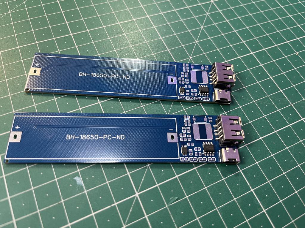
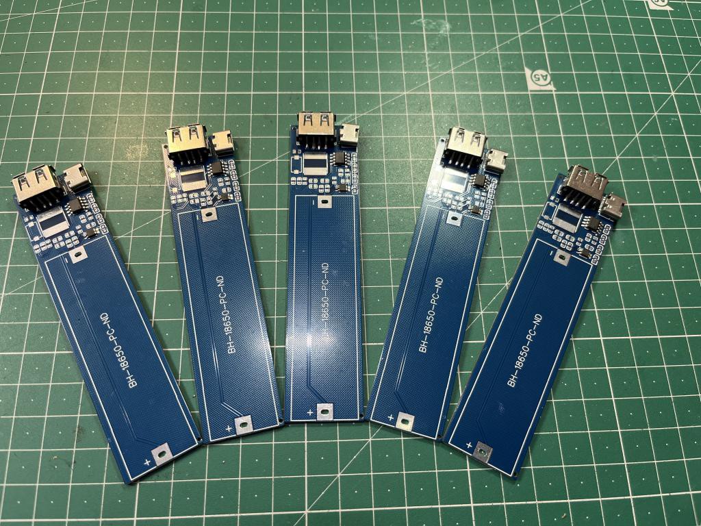
You can check the datasheet from here. The whole setup eliminated the old TP4056 charger, protection and Mt3608 booster out of the circuit very intelligently. here I have 4 more Pieces of assembled boards available for giveaway, just leave a comment below.
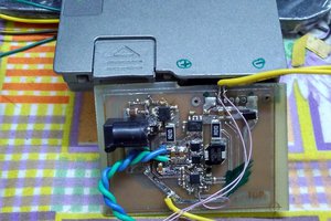
PCB designs and layouts:
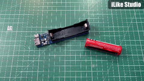
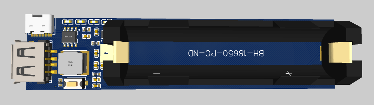
To make it handier I designed the PCB with 18650 battery holder mounted on the top. All the components are place on one side to lower down the SMT assembly cost. A big copper pad to upgrade the inductor with higher value. The circuit is very small but work very efficiently. Get your hands on the Gerber and BOM files from here.
I am using JLCPCB prototyping service in most of the projects because they provide the best quality in a very lower price range. The quality of components and soldering joints is comparable to any supplied with the same product. The price depends on the demand and JLCPCB is the most leading PCB manufacturer from China. Sign-up using this link to get $54 new user coupons and explore more service offered by JLCPCB.
Battery used:
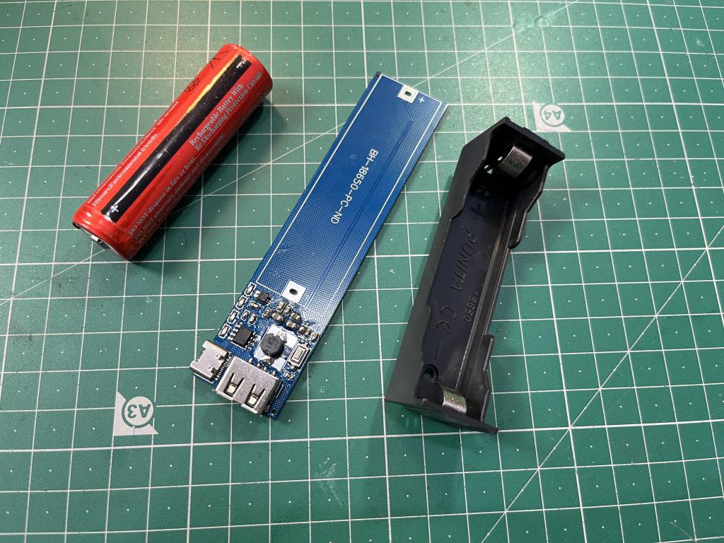
You can make this device using a 4volt lead acid battery, 3.7 Li-Po and li-ion battery. Here I am using 18650 lithium cells. I have 4000MAH power cell which provides a decent battery backup with 90% efficiency rate.
Switch features:
As mentioned...
Read more »
 Justin Maynard
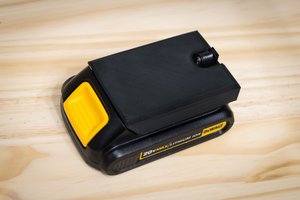
 Vitor de Miranda Henrique
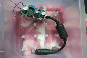
 Kumar, Abhishek