 Dave Collins
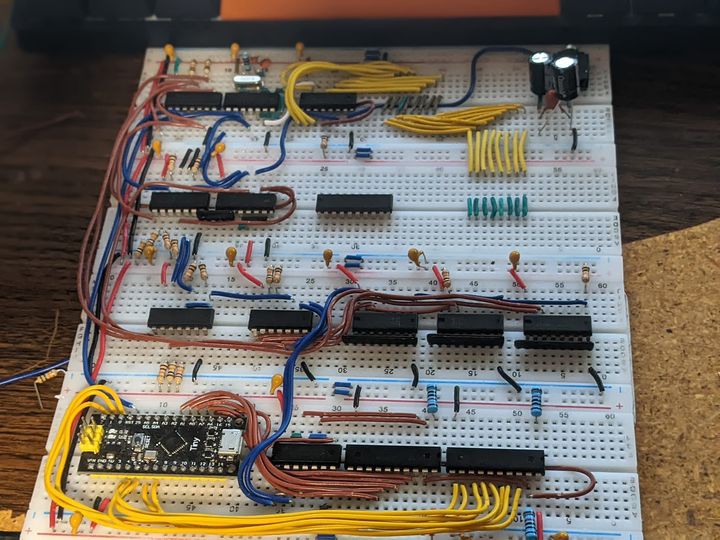
Status:
HBSound development continues, Many have seen this picture kicking around social media. This is what I'm now calling prototype 1. And some of the things I learned from this build are its complexity is it's downfall. When I built the top module I felt it was reasonably successful jumping point because it actually worked. This led me to add in more complexity and, I believe that where the issues started. Prototype 1 used a large NAND to combine all of the output signals, and the ready signals (plus some select able buffered clocks) to make the shift out clock. For a lot of reasons this was a bad Idea. in fact the design was so busy, and chaotic I am hesitant to share it further than the block diagram because, I am afraid in doing so I open up opportunity to optimize a thing which probably is so flawed it should not exist. That being said, in prototype 2 I have to go so much simpler. The first issue is the SN76489, its a wonderful part for its time, but it has some issues which require layers of complexity to over come. Firstly it requires a 3.5-4 MHz clock to create compatibility with period correct machines, most of the source music is written with this timing range in mind and so its a requirement if you want to play music files from other machines that also have this sound chip. The part also has to be silenced from the host machine using initialization. Until then it comes up in a random state and makes noise out of the output. To over come this typically a SR flip flop is used to gate the PSG's clock, this requires more control logic and additional logic to XOR the system reset line which again adds more complexity. This set up allows you to halt the PSG clock but this does not completely reduce the noise from the PSG. The other issue was trying to use the FIFO in a pseudo write - through mode this failed. The timing window was too small, too many signals had to settle in the gate, this created among other things, unreliable timing.
So where does that leave us?
I think I need to take a look at picking one chip for the card and I'm leaning widely towards the DAC. A DAC provides the ability to create very robust sounding output, with digitally generated tracking using spare cycles between operations; there's a large body of sample work as the design I'm shooting for is very compatible with the COVOX / DSS for the PC only with a beefed up oscillator design. Another big benefit is the part is still available on Mouser / DigiKey. The PSG has complications which make it harder to use reliably, requires gated clock generation, that has to be halted to really effectively use it as a select able module, the part also has to be pragmatically silenced in order to really shut down the sound generation completely. Another issue which is a small problem since they are still plentiful the PSG is new old stock.
I think the choice is clear, I should use a single chip DAC and stop messing around with trying to provide a optional write through mode. The 2-32 kHz sample rate (which is software select-able) I'm shooting for is more than enough to produce far better sound quality than even the reference Disney sound source, which had a fixed 7-8Khz sample rate provided through a 555 timer. My design uses a fixed crystal oscillator to produce the base clock and a counter chip to produce the pulses.
I decided this time to build up the control logic in "Digital" logic simulator. Its a nice Logisim clone, that's actually got properly functioning 74254 bus transceivers, which i used HCT variety in my build so I could use faster HC logic and still interface a TTL CPU. You will recognize the Motorola specific architecture signals are used here but the basic design should be able to be adapted to any basic single clock R//W set up.
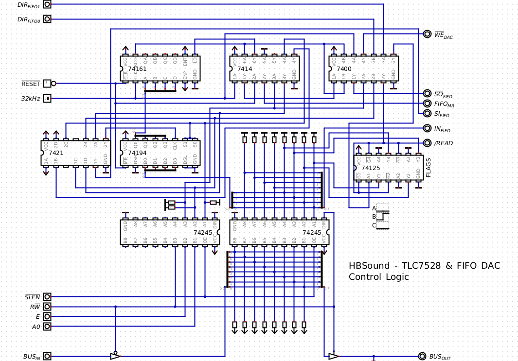
The control logic is 8 chips, most of witch is dedicated to creating the two falling clock edges needed to clock the DAC and the shift out line of the FIFO. Here is a blown out diagram of the functionality of this clock generator:
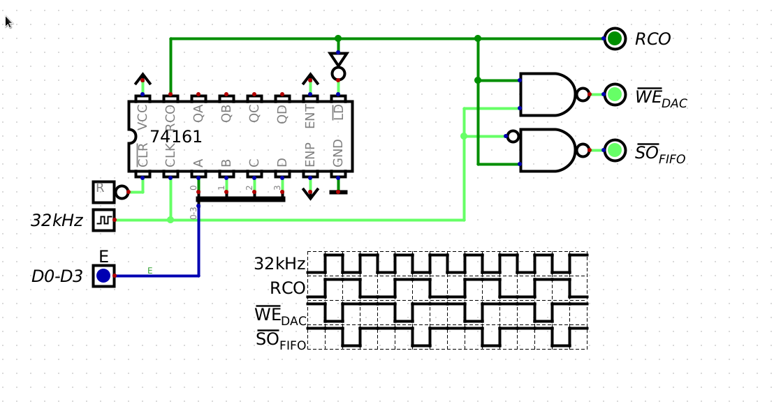
The 4 bit value is loaded into the counter via a universal shift register. The register is wired as a storage register. I used a universal shift register because its Load operation is a high signal on both control pins, which makes building the logic to select which device gets clocked on a write operation much simpler. The basic thing to get your head around and understand is, it provides a parallel 4 bits to the inputs of the counter, and can be set by sending a value to Slot enable + 1 (we abbreviate as SLEN). A quirk of this design verses using a state machine is the active count simply counts up from the set value but only after it is latched in, and that means if a count is started the new value is only valid only after the pulse generation happens. So a programmer will have to wait for the first cycle to pass by burning some cycles to grantee the clock is counting at the desired rate. Once interrupt generation is more clearly defined it will be easier to determine how this looks.
We do a NAND operation on the RCO with 32kHz & /32kHz, the result is 2 falling clock edges on the rising and falling edge of RCO. First we sample the waiting output on the FIFO which is always the current byte needing to be read in, by clocking the DAC, then on the rising edge of the DAC clock we shift out the next byte from the FIFO.
Then I use a 74HC21 and a spare NAND gate, and 2 more inverters to generate the /READ, SI_FIFO, and CLK_CREG signals (not pictured on main diagram but wired to the clock pin on the universal shift register).
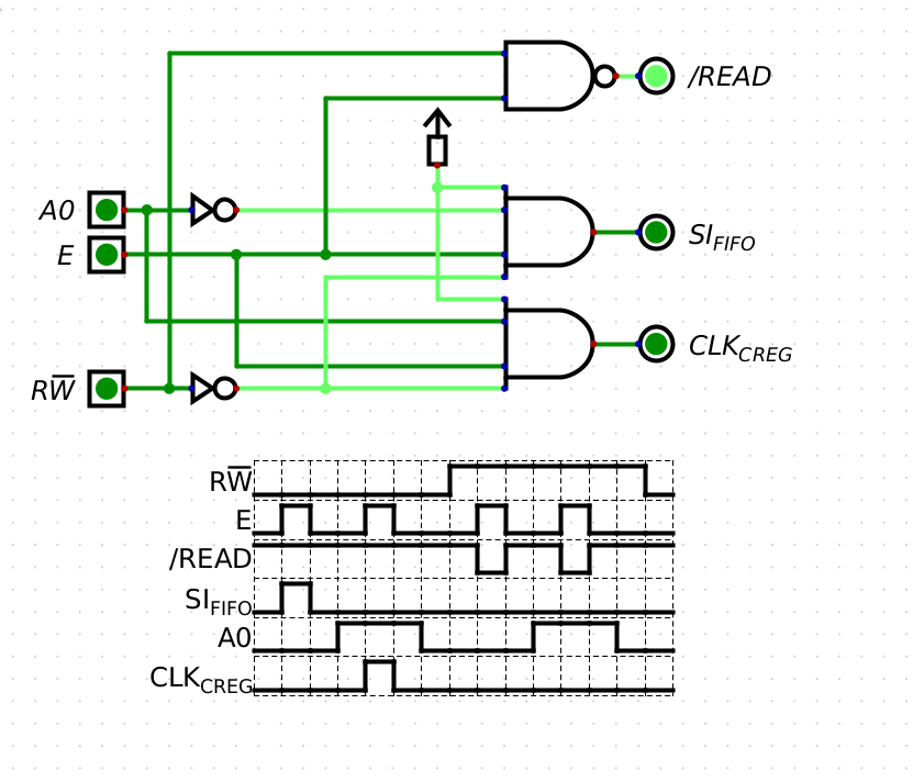
These signals are buffered at the card edge, by a locked direction bus transceiver (the data bus direction on the transceiver for the main bus). the transceivers normalize the TTL signals on the system bus and control lines to a more normal CMOS levels. Oddly enough the Shift in, signal for the FIFO is positive edge triggered, while the shift out signal is falling edge triggered, this was slightly advantageous as the universal shift register is also positive edge triggered.
Buffering the signals and gating the clocks with R//W adds the needed delay to properly clock the data bus in generally a stable state as:
6809 notes
 this is a relatively over simplified assertion but typically in a
 minimal controller based set up:

"e" line goes low ...
 step1                    {address bus updates (addressed transceiver
                          {should turn on if any)
Almost at the same time   {
                          {r//w line (transceiver direction changes
                          {depending on configuration)

   at the end of this transitional step the above signals are in a steady
   state and break down at the next low e transition.


 step2                    {data bus is asserted fractions of a second
                          {before ...
Almost at the same time   {
                          {"{e" line goes high (/write /read at this
                          {point when NANDED with R//W)

  at the end of this transitional step the above signals are in a steady
  state until the end of the next step1 both step 1 and step 2 are at
  in the same states from the end of step 1 until the next
  q pulse (90 degrees later)

while....

q goes high 90 degrees later from e. at approximately the same time as
the step1 and step2 transition

(see diagram on page 9 of the datasheet)

DMA, HALT and other bus control scenarios not taken into account.
Reading out the flag:
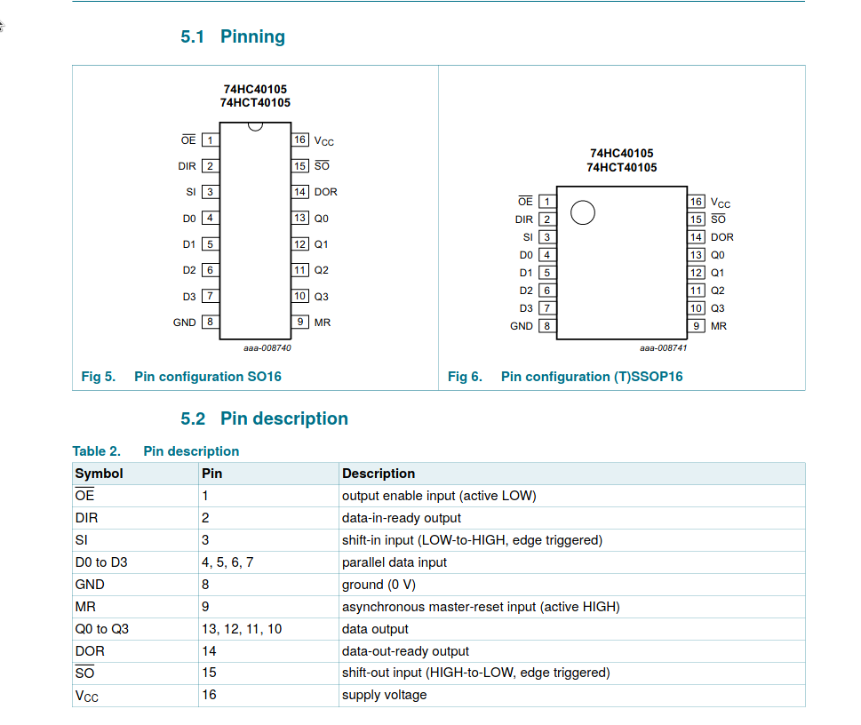
The /READ signal turns on the flags buffer, which currently outputs the NAND of DIR_FIFO0 & DIR_FIFO1. these values are internally latched within the FIFO. This works without the addition of a second latch as the value is valid after the falling edge of the last SI_FIFO signal, which is the case one clock cycle (at least) of E later, when the next /READ signal is asserted. For the interested here is a breakdown of the 74HC40105 FIFO:
 The downside to this means the DOR signals, would absolutely need control logic that would only make the DOR valid to the flags buffer only after the rising edge of the /SO_FIFO signal. Additionally the signals from both chips would have to be fed from an AND gate, as both the DOR and DIR pins go low for a moment as the internal bubble up happens. While this period is fast enough for it to fall between clock cycles from either end of the chip its slightly more difficult due to the way /SO is clocked. Since the input is handled by the system clock the currently latched FIFO value is guaranteed valid because it is impossible to both read and write to the card at the same time, this is not the case with the output side of the FIFO, as it is driven from a separate clock which operates at a much slower rate, that is variable and a trialing pulse to latch the value is not always guaranteed. Generating a latch clock would be tricky as it would need to come after the value on DOR is valid as a buffer is empty signal (vs busy). Simply latching a 74hc74 using the buffered rising edge of /SO_FIFO might work; I may play around with this, as I have at least 2 spare buffers and adding a 74HC74 at this point is trivial. I also intend to generate 2 interrupts from the card, one 32kHz interrupt and one off of the buffered DOR signal from the FIFO. These interrupts will be re-direct able into the IO/interrupt channels on the HB6809 or simply switched off completely.
 Whats next?
Next is the build up of the prototype, I may jump right to spinning up boards for the sound card after I'm confident I can control the DAC using 5 Volts only. So I guess the fist step is getting the breadboard cleared off of the first prototype and hooking the DAC to a micro controller to try to build the analog circuit and get that working.
Discussions
Become a Hackaday.io Member
Create an account to leave a comment. Already have an account? Log In.