 Sagar 001
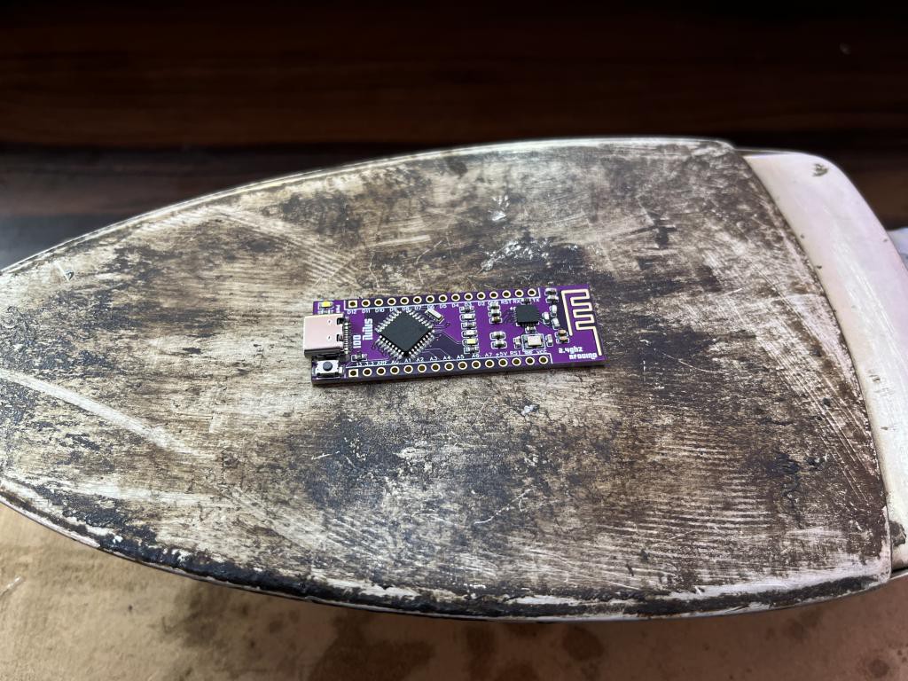
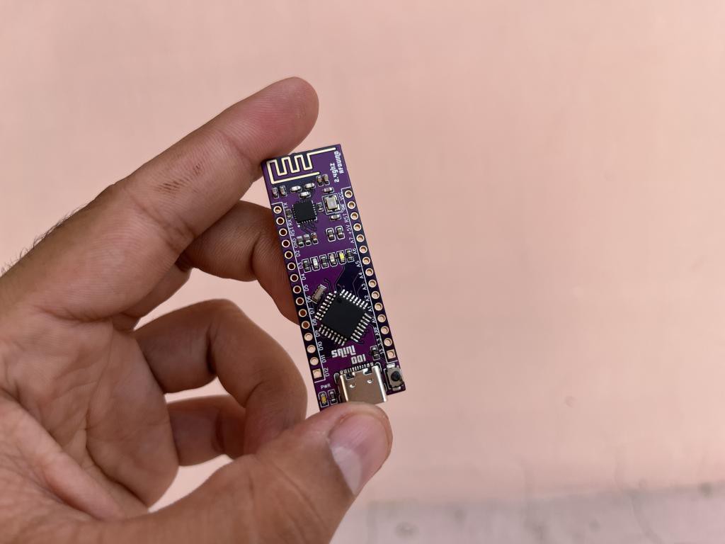
PCB (printed circuit boards) are really very important to minimize the circuit design area and overall cost. PCB manufacturer quality and capabilities depend on the material and minimum featured sized of tracks width. Some of the manufacturers provide up to 6 layers of PCB. I designed and integrated the Arduino NANO with NRF24L01 trans receiver module.
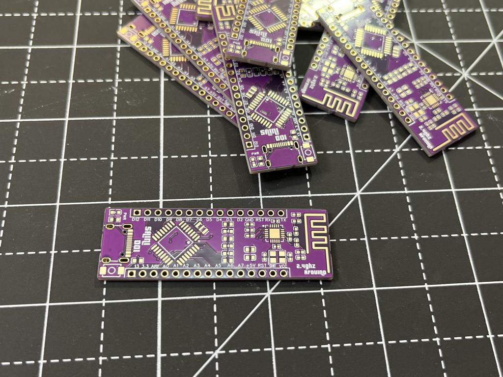
This PCB is made under JLCPCB and assembled manually by me. I have done some minor upgrades to the old Arduino Nano like a type C new Generation port, small crystal oscillator, on PCB antenna and 2.4Ghz radio compatibility. JLCPCB is the China’s leading manufacturer working in the same field for more than 15 years. Sign-up using this link and every new used will get coupons of worth $54.
This Arduino designed is dedicated from the existing ones on the Chinese websites and they are selling them for $40 per piece. But my designed Arduino is very cheaper than that. You can get the PCBs just in $50-60 for 10 pieces of the same board including stencil. Here I don’t have QFN package of Atmega328p that’s why the tracks are very separated to each other and I have to use 6 layers for it.
Components required:
Atmega328p SMD chip
NRF24L01 chip SMD
16MHz crystal
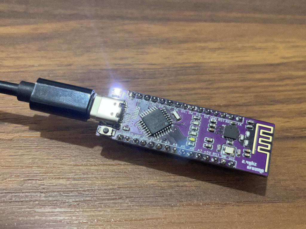
Type C USB
CH340C (USB TO TTL)
100nF, 10nF, 1nF, 100pf capacitors
10k, 1k resistor
Small 0603 led
Reset button
AMS1117 5V
Components from original NRF (Inductor Coils)
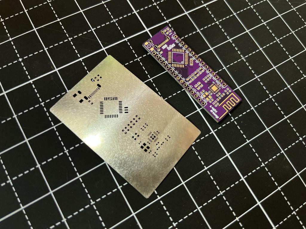
Custom PCB from JLCPCB
Circuit diagram:
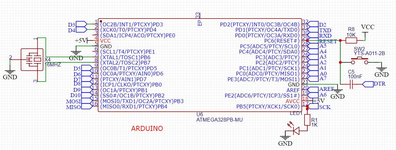
I built a NRF24l01 module for the testing first to know the real schematics of the radio module and then implemented the same on other big form factor board. But keeping the breadboard use in mind this time the form factor is designed same as the NANO. PCB antenna is embedded at one side of the PCB. The microcontroller is made to work independent and can be changed to NRF mode using software chip enable instructions.
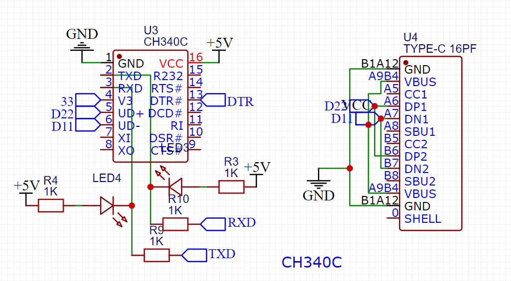
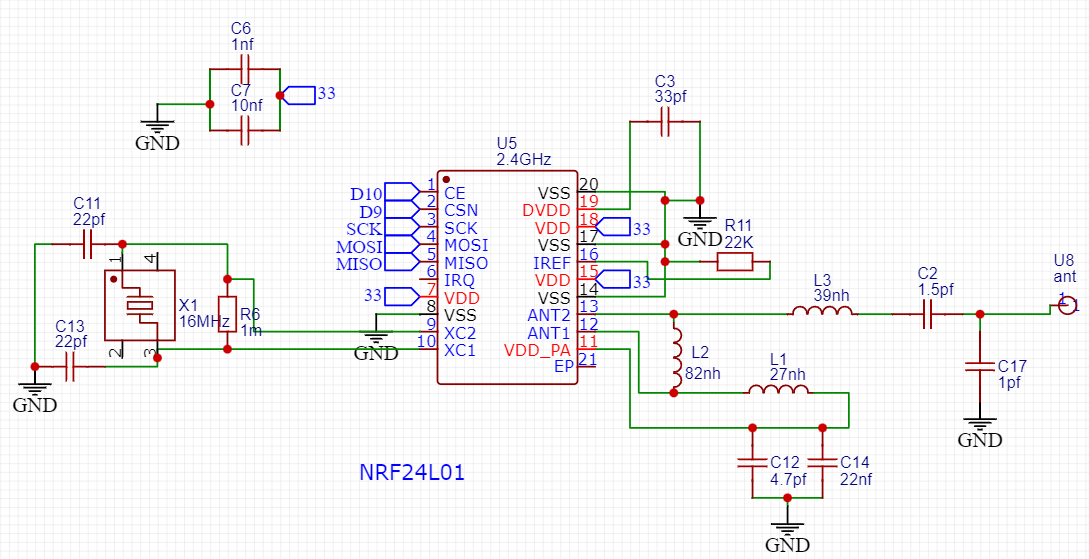
The whole circuit is so connected that the NRF24L01 is connected to the main microcontroller via SPI interface. In this SCK, MISO and MOSI are connected to D13, D12 and D11 pins. CE and CSN pins are programmable according to the schematics but for this CN to D10 and CSN to D9. NRF radio is powered using CH340C on chip voltage regulator and AMS1117 5v regulator for the main Atmega328p microcontroller.
Gerber files and PCB layouts:
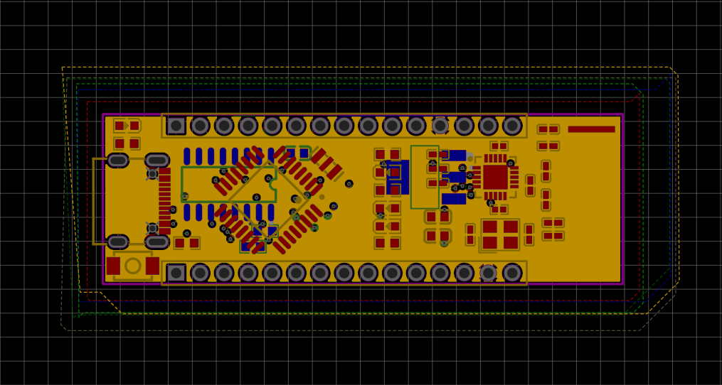
First, I tried to compress the joints and connection in a dual layer board under the JLCPCB capabilities. But due to the big SMD package of ATMEGA328P it is not possible. The QFN package of Arduino chip is not available to me right now. That’s why the PCB got 6 layers if you want to use the same PCB for your design then download the Gerber files from here.
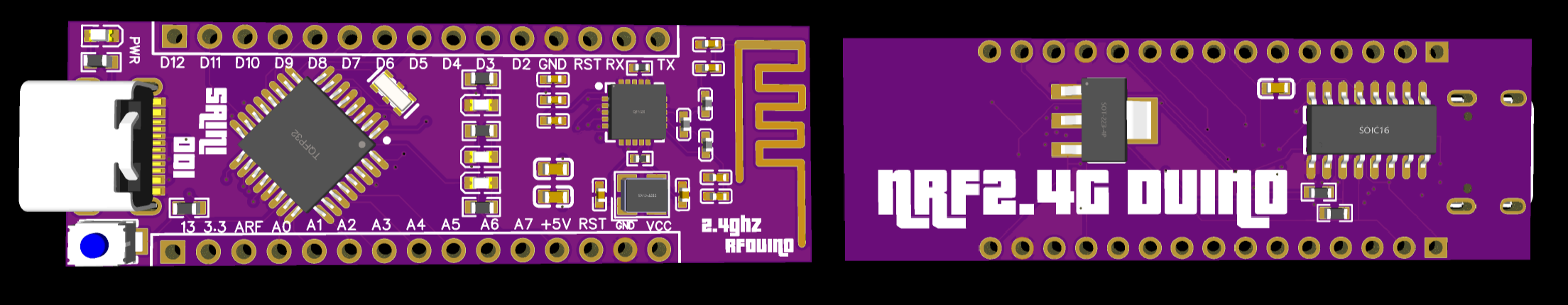
I received these amazing 6-layer purple color ENIG finishing PCBs from JLCPCB just in 7 days after manufacturing. Sign-up to JLCPCB using this link and get $54 new user coupon for the next PCB, SMT orders.
Soldering components:
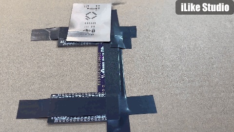
I used SMT stencil service from JLCPCB it will cover a thin uniform layer of soldering paste over the PCB. Then place the parts on the PCB gently, solder using the hot plate or hot air gun. Stencil can be used multiple times using the proper housing. It can be taped using the same PCB housing from 3 sides and PCBs can be inserted from then other side.
First look and testing:
The purple solder mask layer is very good, you need to repair some soldering joints because of uneven temperature curve of solder heater. Nrf24l01 module is embedded at one side which makes it to use independent. After that I will test the microcontroller continuity and then power it up and check the power consumption of the total board.
Programming:
After burning the bootloader, it is always recommended to go with the simplest blink code it will help to check the software and hardware problems. You can see the Arduino bootloader tutorial from here.
Troubleshooting:
The main problem is to solder the type C USB on the PCB because of its small connection points. Power and data lines are connected to the PCB...
Read more »

 Tom Goff
 Jelto
Jelto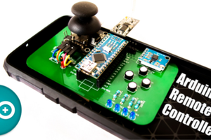
 Jithin Sanal
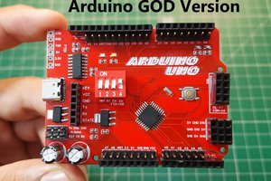
Sorry for the mistake that one is of 16MHz, I will correct the BOM ASAP