You walk into a room and want to adjust some of your smart devices? Pull out you phone, turn on Wi-Fi, find the Home Assistant app and wait for it to load. Search for the right tab and finally adjust your devices.
Way too much work...
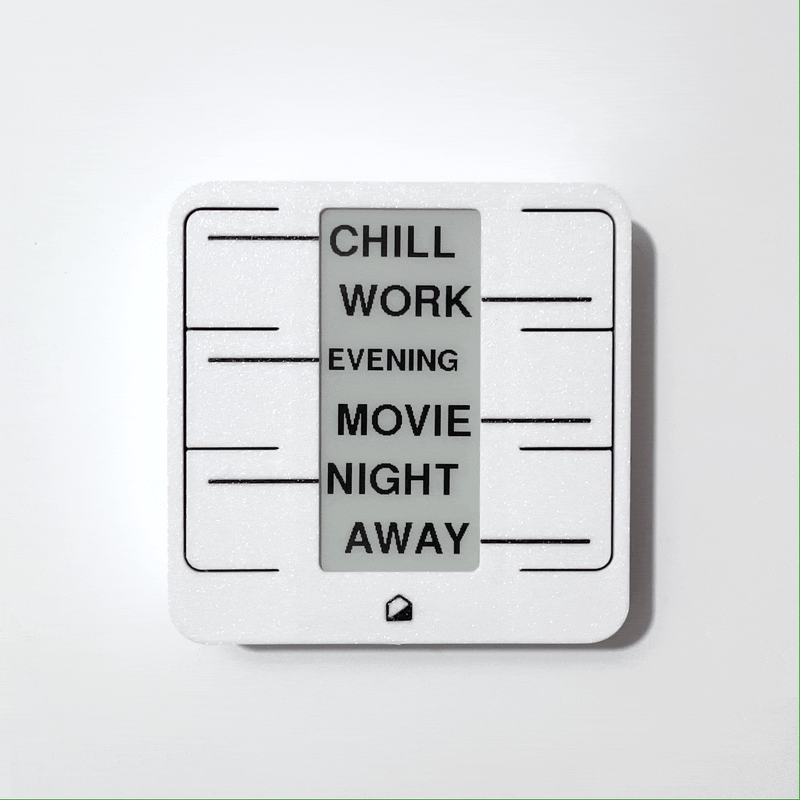
With Home Buttons, quickly activate one of your favourite presets with a touch of a button.
Technical overview
Home Buttons is designed to be as simple as possible for the user. No cables, no charging every couple of days, no absurdly difficult setup, no special gateways needed. How do you design a device like that? And make it feasible for low-quantity production?
Display and buttons
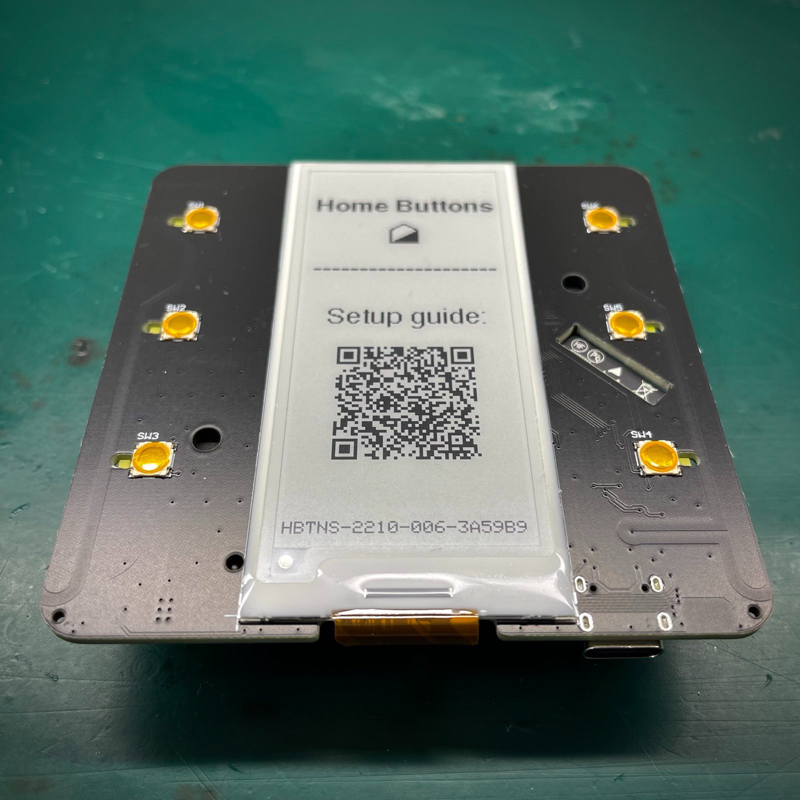
Displaying a short label for each of the buttons was the goal of Home Buttons. A 2.9" E-paper display was selected due to being a very nice and readable size, consuming zero power while displaying an image. It also looks amazing and unobtrusive, being lit by the environment, not emitting light itself.
Number of buttons was selected to be six, a compromise between providing enough shortcuts and device not being too crowded. ALPS SKRB pushbuttons were the perfect choice, providing satisfying feedback, but also being very low profile.
Each button has a white LED beside it. It illuminates when a the button is pressed. Reverse-mount LEDs are used, so they can be machine assembled on the side of the PCB where all of the electronics are.
Energy limitations
Obviously, Home Buttons should be battery powered and connected to Wi-Fi. But Wi-Fi connectivity comes with relatively large power requirements, which was a major consideration during the design phase.
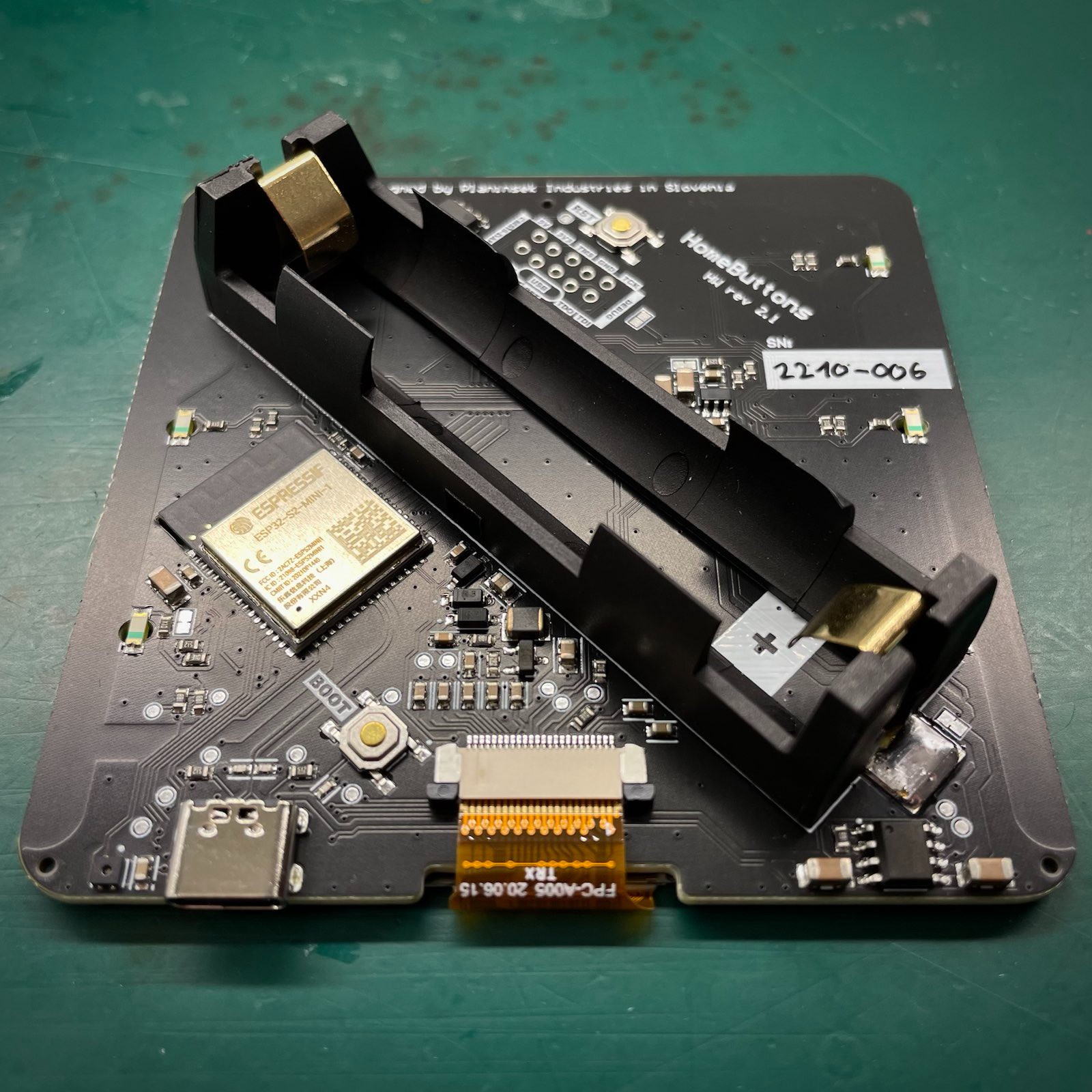
- A high-capacity battery is needed. 18650 size is an easy choice, providing lots of energy while being common.
- E-paper display draws basically no power when not updating.
- ESP32-S2 SoC is a good choice, being inexpensive and offering excellent sleep capabilities.
- A low power temperature and humidity sensor is used.
- Voltage regulation is carefully designed to maximize battery life, while reducing self-consumption as much as possible.
This way, Home Buttons last more than a year of frequent usage and temperature / humidity reporting on a single charge. Charging is of course done through a USB Type-C connector.
Voltage regulation
This is a complicated one. Battery voltage can be anywhere between 4.2 V when fully charged, down to around 2.8 V when fully discharged. But the ESP32-S2 needs a stable 3.3 V. It can also pull bursts of more than 300 mA. This is not trivial to put together, especially while having a very low quiescent current necessary for battery operation. And the chip shortage does not help!
After a few iterations, the final version uses a very good LDO regulator, set at 3.1 V, which is still in spec for the ESP32-S2 but enables a deeper discharge of the battery then setting it at 3.3 V. The battery discharging limit is still set at 3.3 V to account for the dropout voltage, which can get quite high when Wi-Fi communication is active. For most LDOs the drop could easily be more than half a volt, making them unusable. Discharging only to 3.3 V is a compromise which leaves some capacity in the battery. But it makes sense, considering the complexity, cost and quiescent current of other options. Texas Instruments makes some really nice buck-boost converters exactly for this, but of course at the time of development, they are not even close to being available.
Environment sensing
It makes sense that a fancy smart and connected device has a good temperature / humidity sensor. Not only is it nice having a reliable temperature reading, it can also be used in climate control automations. Sensirion SHTC3 is a great choice, being accurate to +-0.2°C and also having a really good sleep mode.
Battery management and charging
For safety, lots of protection is needed. An integrated protection IC takes care of the general overcharge, overdischarge, overcurrent, etc. There is also a single-mosfet reverse polarity protection, so the battery can be inserted the wrong way without anything scary happening.
Charging is handled by the cheap and reliable TP4056 linear charging IC powered from the USB Type-C connector. It takes around 4 hours for a full charge, but does it really matter if charging is needed less then once a year?
Proximity sensing
At the edge of the PCB, a proximity sensing strip is integrated. This makes use of the touch peripheral of the ESP32-S2 and looks very promising in testing, but is not yet implemented in firmware. Once it is, LEDs under the buttons will light up when you move your hand close to Home Buttons, making hitting buttons in the dark much easier. Coming soon via software update :)
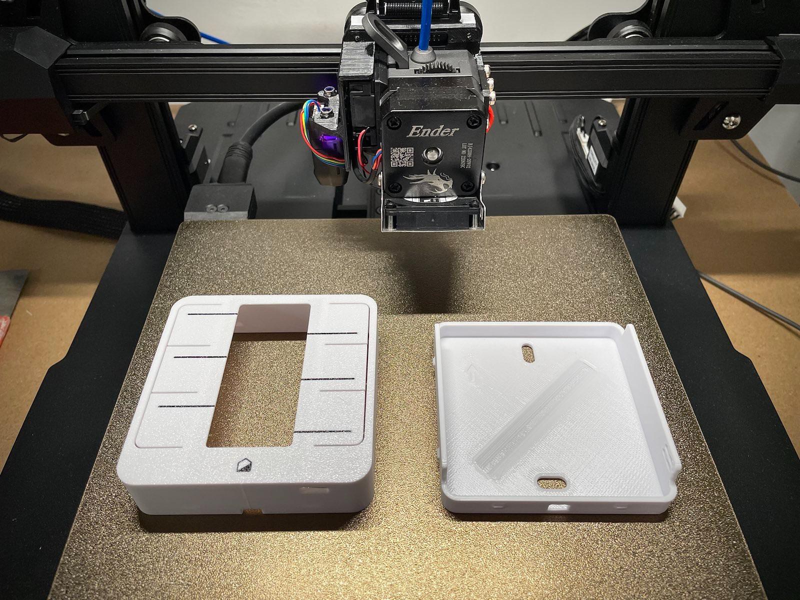
Case
For a small production run, 3D printing makes the most sense. Cases are printed on a normal FDM 3D printer, using PETG filament. To get graphics on the front, the white part of the first layer is printed first, then the filament is swapped with a black one, filling in the gaps. Filament is swapped again and the rest of the case is printed in white.
Manufacturing
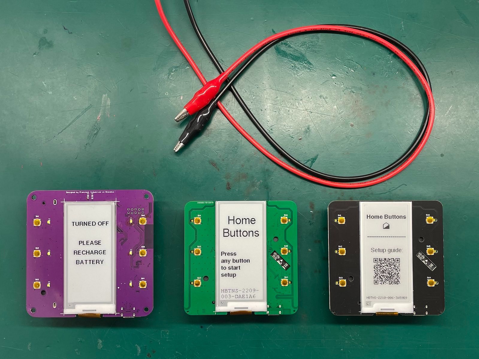
A huge part of the design is making Home Buttons easy to manufacture. PCB is made and mostly assembled at JLCPCB and is optimised specifically for their process and selection of parts that are already preloaded in their pick-and-place machines. To reduce cost, the battery holder and buttons (which are on the other side of the PCB, making it a double-sided load) are assembled manually. After this, the display is added and the board is tested carefully and programmed. Next, cases are 3D printed, checked for adequate quality and the PCB is inserted, making Home Buttons ready for use.
Specs
A full spec sheet is available at https://docs.home-buttons.com/specs/.