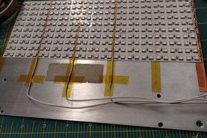
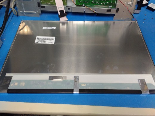
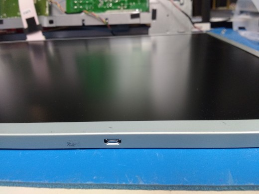
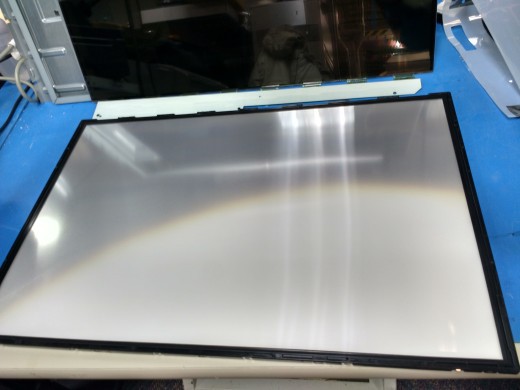
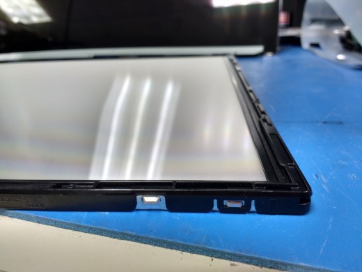
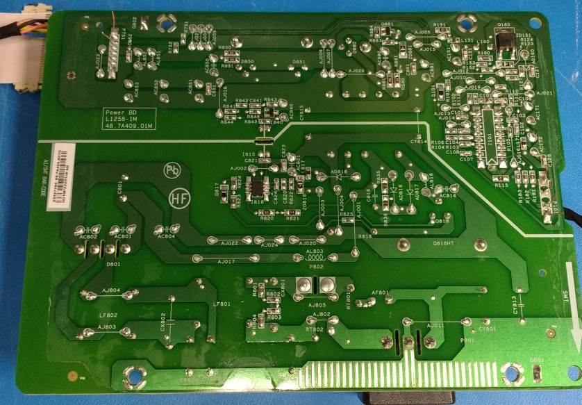
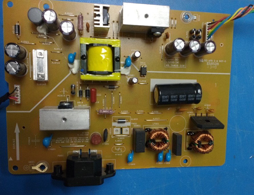
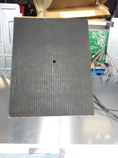
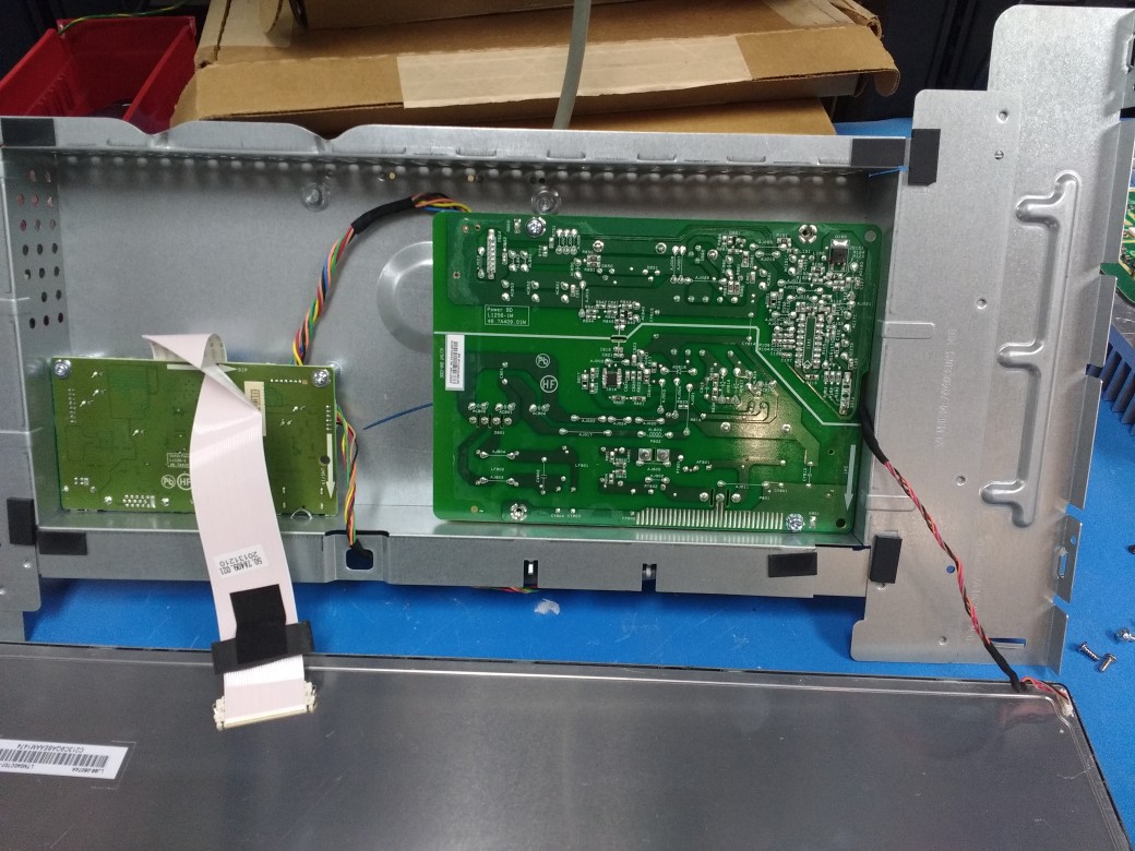
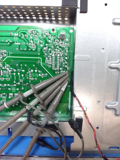
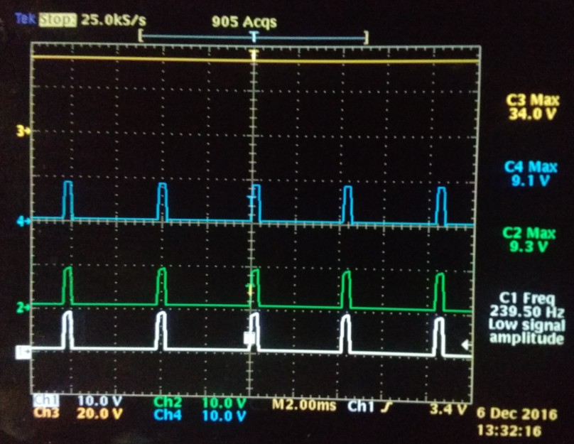
Close
0%
0%

LCD light box conversion

A quick "afternoon" project with a scrap monitor.

Similar projects worth following
I've seen this project done by others over the years, and wanted to make one of my own, but had just been waiting for a good enough display to use. The panels on laptops are rather small, so I was looking for a larger, and more modern display, preferably with LED illumination instead of CFL. I stumbled across a recent 24" 16:10 monitor in the scrap bin, and decided it was finally time to do it. This is a monitor which is large enough to light an entire 11x17 page, with an illuminated area of 20.5 by 12.8. I also wanted to make this a quick project as they are rewarding to start and finish something so quickly.

This project uses a scrap HP LA2405x(24" LED lit LCD monitor) that has failed, and repurposes it as a light box for tracing. The end result uses the original monitor frame and bezel, with an overlaid glass to provide strength against the surface.

  • Disassembly of the panel

    Quinn12/07/2016 at 03:28 0 comments

    LCD panels are complicated stacks of parts, with many times awkward clips and adhesive holding things together. I've taken apart a lot of them before, and while there are some similarities, there are also a lot of differences, especially the way the backlight itself works. Having the disassembly instructions intended for someone recycling the monitor helped confirm the process, but it was not a surprise.

    First was to pull off the plastic sheet protecting the circuit board. It is attached with simple adhesive, pulled off gently.

    Next was removing the outer frame, which was clipped in along all the edges.

    These were pretty easy to slip a slot screw driver between the frame and the inside, lift the frame out a little, and apply pressure to push the frame away. The first one or two were tricky, but after a couple came it was really easy.

    Here I had to do the bottom and sides, because the top had a metal lip around the backside. Once the bottom and sides were done, the frame simply tipped up, releasing the top. In this case, the panel was now free, save for the adhesive that attached it to the inner plastic frame. Applying gentle but constant pressure to pull the panel off the frame using a corner, it slowly lifted free without breaking. In the below picture, the LCD is in the background, leaning against some boxes.

    This next picture shows the clips attach. The left one was for the outer frame. The right one is for the inner plastic frame. If I wanted to pull apart the diffusers, I would lift out those clips to separate the frame.


    At this point, I've done all the disassembly that should be needed. This was one of the easiest panels I've taken apart, which was nice. I snapped the metal outer frame back on, and tested it out. On this panel, because there was the inner plastic frame, I could do this straight away without the backlight diffusers falling out. In other panels, they may, and you will need to come up with a spacer, or just replace the LCD panel with the same size clear glass. I could have taken it apart further, by my experience with panels is that they don't always go back together perfect, and the further you go, the more risk you have. As I actually want to use this, I stopped here. If you have a scrap monitor you don't want to use, go ahead, the layers in the diffuser are fascinating material.

    Testing it proved plenty bright now that the light didn't have to go through the dark LCD polarizers and glass layers. I know that backlights focus the light in a specific angle so as to not waste light. I found that the viewing angle of equal light was slightly larger and similar to what it was with the monitor fully assembled and working. In this case, plenty of working room when working from above the light table. The original monitor specs were "Up to 170° horizontal and 160° vertical", though in practice, as a functioning monitor, I found it to be narrower. I think with the LCD removed, it seemed pretty close to this.

    Next up is to decide how to protect the surface.

  • Reverse engineering cont

    Quinn12/07/2016 at 03:08 0 comments

    This does call into question what the three lines to the backlight are. Perhaps they are not RGB, but instead are just different segments of the backlight. My first thought was to quick pull off one of those resistors and see how it changed, but remembering that they are glued down meant that was going to be a bit harder, and may damage the component. Instead, I simply used a bench supply at 30V, set to 30mA, and some a pair of DMM probes touching the connector pins briefly to see what happened. Indeed, the three lines appear to be different segments of the backlight. Bottom of the power board showing the backlight connector at left with pigtails attached. At upper left is the connector which goes to the control board.

    It's a bummer, but understandable. My guess as to why there are three lines is so that the LEDs are not in parallel, but instead three series chains. Adding them all in series would have required over 90 volts, so this is a likely trade off. They could have added the resistors on the backlight boards themselves so that they would only need a single power pair(as is done when you purchase strips of LED lights), but maybe there is a reason they couldn't do that on the backlight board. I might find out when I take apart the panel itself. Power board top side:

    The curiosity got to me, and I did in the end unsolder the driver heatsink to find out it is a OZ9998BDN. The only available data I could find on it is a quick datasheet, which indicates it is a 4 channel LED driver chip. As noted there, a good reason for spliting the strings into multiple is that it can operate even if one LED fails, leaving the other two strings working. As it is just a quick sheet, there are no electrical numbers, but thankfully there is an example circuit with pin numbers. That said, the pin numbers do not match, but the part is available in multiple packages, so that could be the discrepancy. Regardless, the example confirms the updated theory as it has an ENA and an PWM input. It also makes it clear that this chip itself is controlling a boast converter to supply the 34V. I can also compare the example and identify the key components in it.

    Anyway, I put on some new thermal compound, soldered the heatsink back, and reassembled all the boards into the chassis, testing again that it does in fact, still work. Next up is to remove the LCD itself from the frame, leaving just the backlight.

  • Scope pictures

    Quinn12/07/2016 at 02:48 0 comments

    You may have noticed that my scope pictures are from an older scope with a CRT, and are pictures of the screen. This scope does not have an easy output method(only floppy, which I would then need to find a computer with a floppy drive, or GPIB, which is a lot more work than it is worth to setup and requires extra software). Instead, it is a camera picture of the screen. Anyone who has done this has found that reflections of room lights etc often show up in the image, but not in mine. The way I do this is that I have a piece of black cardboard, with a small hole cut out of it. I place the camera against the cardboard, lens pointing through the hole, and take the picture that way. The cardboard blocks reflections.


  • Reverse engineering

    Quinn12/07/2016 at 02:41 0 comments

    Powering it up again, I used a multimeter to measure the pins on the backlight connector. I didn't know which pin was ground, so I started by using the metal frame, and found a small voltage on 3 of the lines, and 34V on the last. Trying to measure the lower voltage lines better, I could tell the meter was going up and down, suggesting that they were not DC signals.

    I disassembled it even further to access the main PCBs, in particular, the power PCB9on right below) which the backlight cable went to.

    It is a simple single sided wave soldered board (as evidenced by the backside surface mount components having been glued on, as well as the liberal solder on many pads) which was easy to start tracing. The line I measured 34V on went to some larger electrolytics, with the other side of it going to a ground trace. I could tell the ground trace because it went to a mounting hole to connect it to the metal internal frame. Likewise, I could see that the AC power ground connected to the internal frame. This is a good grounding design principle, so that was nice to see.

    The other three lines went through resistors I measured at 3.9ohm, and to a DIP chip. The chip had a heatsink on the top side, so I couldn't easily read it's part number, but this gave me some major clues. My hypothesis is that this is a open drain driver chip, and the three channels are red, green and blue. This could in theory adjust the backlight color, which enables some nice additional features.

    Anyway, I wanted to confirm, so pulled out a scope. I soldered some quick pigtails onto the 4 pins of the backlight connector on the power board, and clipped scope probes to them, set suitable for handling the 34 volts. With the power board screwed back into the chassis to provide grounding, I grounded the probes to the metal chassis.

    Sure enough, the one line has a stable 34VDC(ch3 below) on it. The other 3 had a 240hz square wave on it, with 340us high time and 3840us low time, further supporting that it is duty cycle controlled, and this was the max default at 92% on time(ch1, ch2, ch4 below). The low side of the signal measured about 0.7V, and the high side about 9V. This suggests the low current drop voltage through the LEDs is 34 - 9 = 25V. Moving a probe to the other side of the 3.9ohm resistor confirmed that the chip side was 0.3V. From this point, I have the specs I need if I'm going to replace the driver. I supply 34V to the high side line, and a OD driver to the others through 3.9ohm resistors. It looks like each line pulls about 100mA.

    That said, I have a perfectly good power supply and driver chip on this board already, so it seems logical to poke around and see what else I can figure out. The connector leading to the logic board has very few signals on it, a ground, another power, which measured at 5.1V, and two signals which measure on the DMM as 2.8V, which seem to be logic lines which go towards the backlight driver chip. When the monitor goes into sleep after about 20 seconds, I can see that the 5.1V rail stays up, but the 34V rail does not, floating down to 24V. (it probably only floats to 24V because of the drop of the LEDs, and there being no other load on that rail) It is an easy hypothesis to make that the other two lines are I2C running at the common 3.3V. This is because there needs to be more than basic control into that driver chip if the backlight is to be controlled via software.

    Adding some pigtails and probing those two lines reveals this not to be the case, which is unfortunate. Trying different on/sleep/off states, as well as triggering on the lines shows that these are not I2C, but instead the first appears to be a 3.3V logic level enable (active high), and the second a 3.3V logic level PWM control(active high for on) as it matches the period, frequency and is synchronous to the LED driver lines. It is interesting that when in sleep mode, the PWM signal is driven at 120hz, but the same duty cycle, not sure why that is. Below plot shows the enable line...

    Read more »

  • Disassembly

    Quinn12/07/2016 at 02:34 0 comments

    The display was easy enough to removed from the stand, but there were no other apparent screws to open the plastic shell. I checked under the rubber bumpers at the bottom where such is often hiddent, but there were none there. I ran my fingernails across the label sticker on the back another common place to hide them. I did find one depression near the middle. Though not optimistic, I cut through the label with a knife, to find what I kinda expected, it was just a plastic molding depression.

    I was going to proceed with the usual flat blade prying between the plastic halves along the edge, but before doing so, a quick google search for "LA2405x disassembly" resulted in this document from the manufacturer:
    http://h22235.www2.hp.com/hpinfo/globalcitizenship/environment/productdata/Countries/_MultiCountry/disassembly_monito_2012417235645.pdf


    It is a disassembly guide for recycling companies to know how to remove parts for recycling. It doesn't show all the key steps in detail, and it uses slightly destructive means, but the pictures did help. I could identify in them that the front and back plastic were indeed just attached with tabs and hooks as is common on such plastic assemblies.

    Prying around, I was able to slowly get the plastic tabs apart. This freed the internal assembly which was not attached to the plastic at all, except for the wire leading to the front panel controls. Both the front and back plastic came off at that.
    Disassembled, I could clearly see the LVDS data cable going to the panel, and a separate cable going to the backlight. As this backlight powers up, I wanted to stop here in my disassembly to make some measurements in order to determine how to drive the LEDs.

  • The source monitor

    Quinn12/07/2016 at 02:29 0 comments

    This project started when a suitable monitor was found in a scrap bin. In this case, an HP LA2405x LED backlit 24" monitor. It was labeled "bad". Powering it up confirms that the actual display wouldn't drive from a computer source, or even the on screen display. However, the backlight worked, which made it a perfect one to use.

    If the backlight didn't work, I could still have used it, but it would have been harder to figure out the backlight LED drive specifications.

    But my experience disassembling LCDs shows that all sorts of surprises can be found which makes the unit harder to use. Need to take it apart to find out.

View all 6 project logs

Enjoy this project?

Share

Discussions

Similar Projects

Does this project spark your interest?

Become a member to follow this project and never miss any updates