 Quinn
QuinnPowering it up again, I used a multimeter to measure the pins on the backlight connector. I didn't know which pin was ground, so I started by using the metal frame, and found a small voltage on 3 of the lines, and 34V on the last. Trying to measure the lower voltage lines better, I could tell the meter was going up and down, suggesting that they were not DC signals.
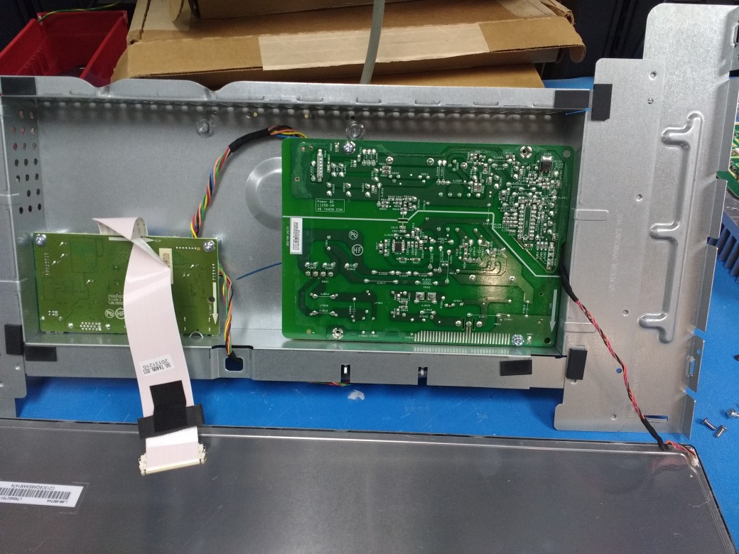
I disassembled it even further to access the main PCBs, in particular, the power PCB9on right below) which the backlight cable went to.
It is a simple single sided wave soldered board (as evidenced by the backside surface mount components having been glued on, as well as the liberal solder on many pads) which was easy to start tracing. The line I measured 34V on went to some larger electrolytics, with the other side of it going to a ground trace. I could tell the ground trace because it went to a mounting hole to connect it to the metal internal frame. Likewise, I could see that the AC power ground connected to the internal frame. This is a good grounding design principle, so that was nice to see.
The other three lines went through resistors I measured at 3.9ohm, and to a DIP chip. The chip had a heatsink on the top side, so I couldn't easily read it's part number, but this gave me some major clues. My hypothesis is that this is a open drain driver chip, and the three channels are red, green and blue. This could in theory adjust the backlight color, which enables some nice additional features.
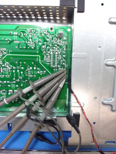
Anyway, I wanted to confirm, so pulled out a scope. I soldered some quick pigtails onto the 4 pins of the backlight connector on the power board, and clipped scope probes to them, set suitable for handling the 34 volts. With the power board screwed back into the chassis to provide grounding, I grounded the probes to the metal chassis.
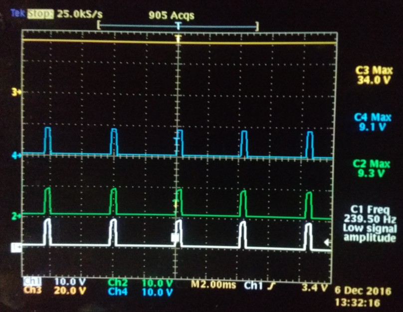
Sure enough, the one line has a stable 34VDC(ch3 below) on it. The other 3 had a 240hz square wave on it, with 340us high time and 3840us low time, further supporting that it is duty cycle controlled, and this was the max default at 92% on time(ch1, ch2, ch4 below). The low side of the signal measured about 0.7V, and the high side about 9V. This suggests the low current drop voltage through the LEDs is 34 - 9 = 25V. Moving a probe to the other side of the 3.9ohm resistor confirmed that the chip side was 0.3V. From this point, I have the specs I need if I'm going to replace the driver. I supply 34V to the high side line, and a OD driver to the others through 3.9ohm resistors. It looks like each line pulls about 100mA.
That said, I have a perfectly good power supply and driver chip on this board already, so it seems logical to poke around and see what else I can figure out. The connector leading to the logic board has very few signals on it, a ground, another power, which measured at 5.1V, and two signals which measure on the DMM as 2.8V, which seem to be logic lines which go towards the backlight driver chip. When the monitor goes into sleep after about 20 seconds, I can see that the 5.1V rail stays up, but the 34V rail does not, floating down to 24V. (it probably only floats to 24V because of the drop of the LEDs, and there being no other load on that rail) It is an easy hypothesis to make that the other two lines are I2C running at the common 3.3V. This is because there needs to be more than basic control into that driver chip if the backlight is to be controlled via software.
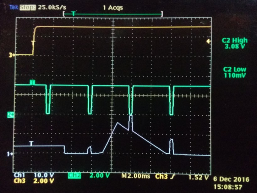
Adding some pigtails and probing those two lines reveals this not to be the case, which is unfortunate. Trying different on/sleep/off states, as well as triggering on the lines shows that these are not I2C, but instead the first appears to be a 3.3V logic level enable (active high), and the second a 3.3V logic level PWM control(active high for on) as it matches the period, frequency and is synchronous to the LED driver lines. It is interesting that when in sleep mode, the PWM signal is driven at 120hz, but the same duty cycle, not sure why that is. Below plot shows the enable line on channel 3, the 3.3V PWM control on channel 2, and the LED driver output(after the resistor) on channel 1.
Regardless, using the power board, I could power and drive the backlight, and have easy PWM control and power enable control.
Discussions
Become a Hackaday.io Member
Create an account to leave a comment. Already have an account? Log In.