These boards have been intriguing me for a while, since they clearly came from a computer system, but all I had to go on was the part numbers printed on the boards. I am fairly certain now that they belong to a Varian 401 or 402, which was a lab data system used to control chromatography machines. Since it is just a Z80 on a backplane, however, it should be possible to replace the ROMs with some new software and have a working computer.
What I Have
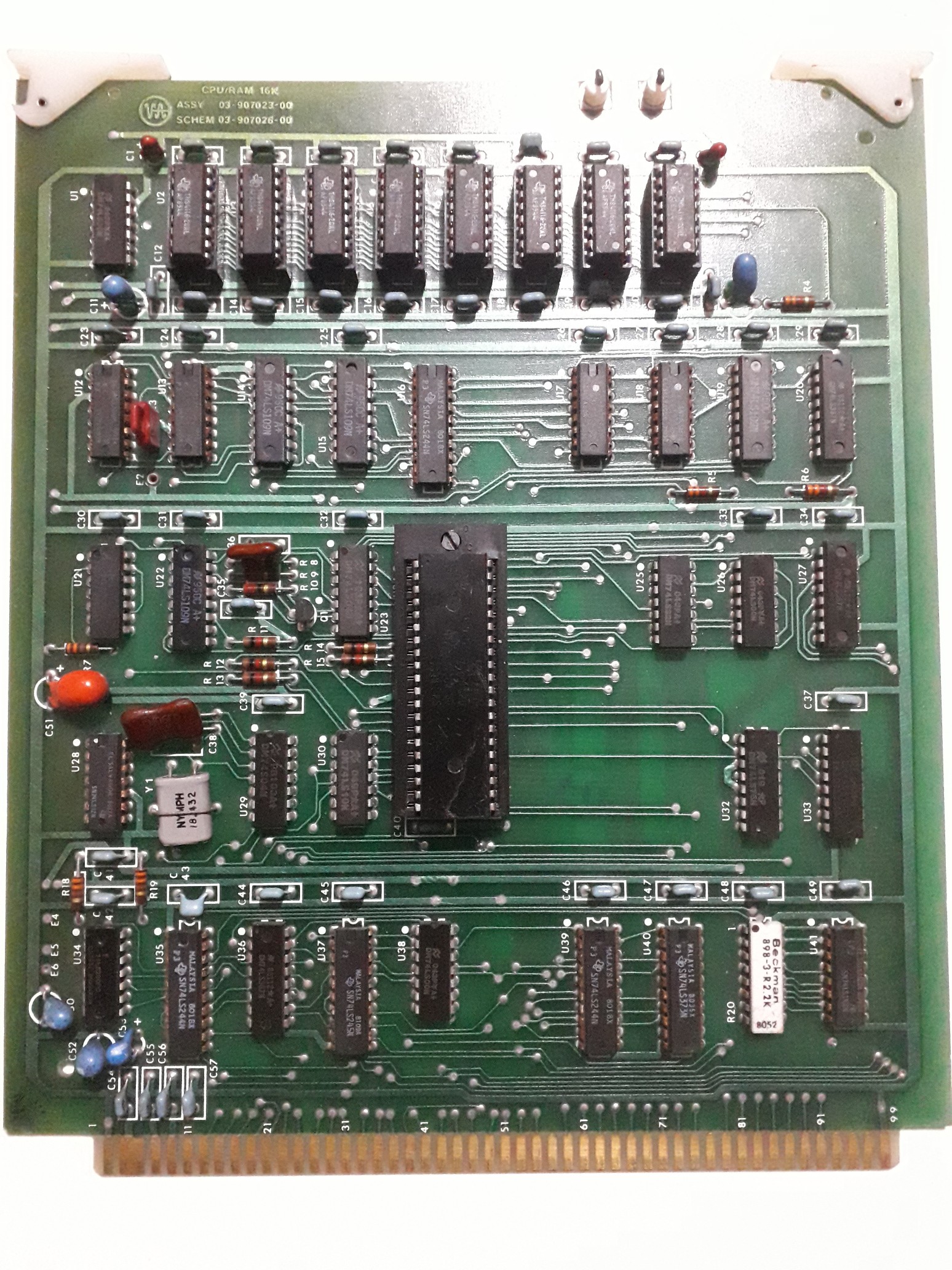
1 x 03-907023-00 CPU / RAM 16K
1 x 03-907013-02 RAM Board
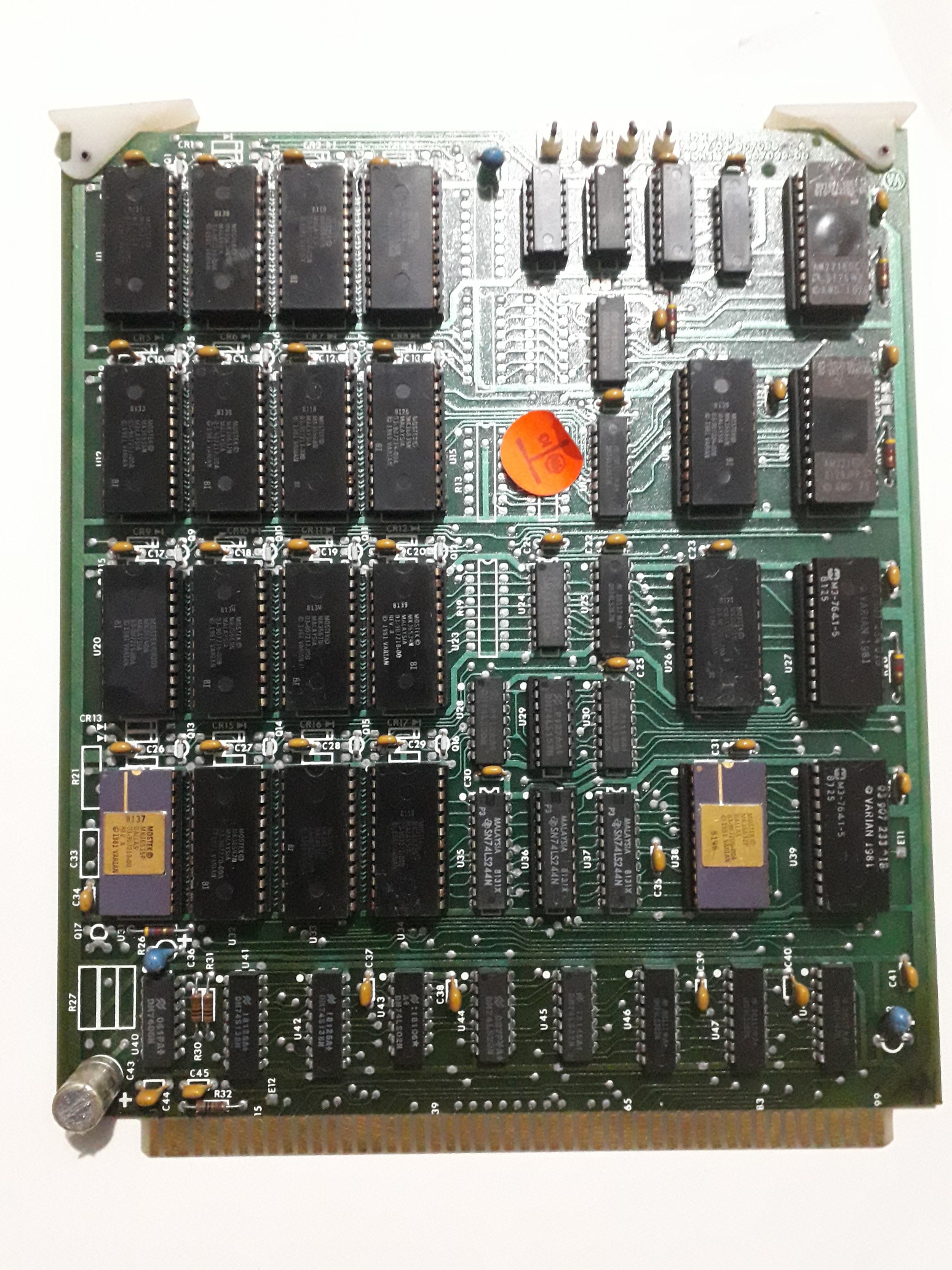
1 x 03-907096-01 ROM PCB
1 x 03-907034-00 CRT And Keyboard
1 x 03-907039-00 Auto Sampler External Events Board A
1 x 03-907006-00 Disc Interface
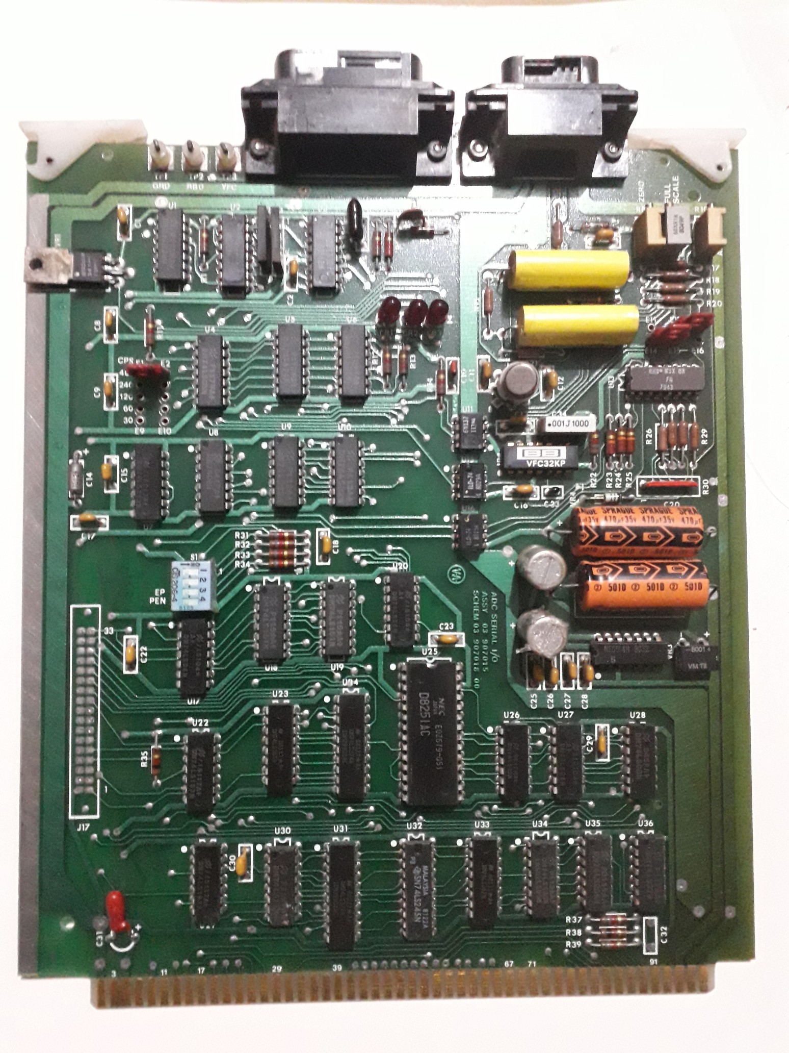
4 x 03-907015-00 ADC Serial I/O
The (vague) plan is to work on the CPU board first, as this should be a self contained unit, then the ROM board and one of the serial boards to try and get it talking. If I can get it working to that stage, the extra RAM can be looked at, then the CRT/Keyboard, and the Disc Interface. The Events board is lowest priority.
What I Don't Have
The backplane - there should be a board to connect all these together, so I will need to work out the pinout of each card and engineer a replacement.
The power supply - The CPU board has +12V, +5V and -5V rails for the DRAM, so I will need to acquire a supply that can generate these, or build one into the backplane. There may be other rails needed for the serial cards.
The CRT - While I have the CRT controller board, I don't have the actual CRT. I'll need to sort out some kind of display or video output eventually.
Schematics or Manuals - Everything will have to be worked out from scratch.
Z80 experience - I'm more of a 6502 person, so I'll have to learn some Z80 assembly for this machine.
Why Am I Doing This
Because I like to tinker, and it seems a shame to just strip the boards for parts if I can make something from them as-is.
 Keith
Keith
 Trevor Johansen Aase
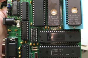
 Craig
Craig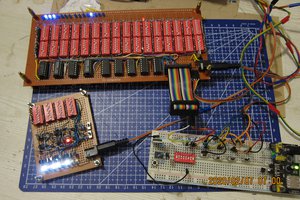
 Pavel
Pavel