 Alan
AlanI know there are many ways to design an MDI circuit.
There's been a lot of discussion and answers about circuits, but I haven't been able to find a really clear and unambiguous answer.
So I decided to run the test.
I tested it with the previously designed W5100S-EVB-TEST board.
Wiznet W5100S-EVB-TEST board production record
The above link is the development process of the "W5100S-EVB-TEST" board.

W5100S-EVB-TEST-V1.0 Board Circuit Cross Section

W5100S-EVB-TEST Circuit Schematic
Let's look at it with an uncomplicated block diagram.
The PHY chip is divided into two modes: current mode and voltage mode.
- Current mode has no DC bias voltage inside, so it must be caught externally.
- Since Voltage Mode has a DC bias voltage inside, there is no need to hold the bias voltage from the outside. (Voltage Mode and Current Mode each have their pros and cons, but Voltage Mode is overwhelmingly superior in terms of power)
I saw an article explaining Current Mode as Open Collector and Voltage Mode as Push-Pull, but it seems different for each PHY.
Since W5100S PHY is in Current Mode, it is necessary to hold the bias voltage from the outside. On this board, all center taps are connected to 3.3V. The voltage applied to the center tap becomes the bias voltage, and it comes out as a complementary waveform around that voltage.
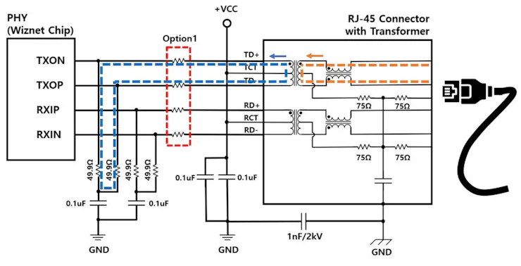
Figure 1 <100 Ohm Termination of Differential-Mode Signals>
[Figure 1]
Here, the 49.9 ohm resistor of the differential pair line that looks like a pull-down is a parallel termination resistor. Since each differential line is very high frequency, + and - change very quickly based on the center tap power. Due to this, the current is not circulated well, so it is reflected and ringing can occur. To prevent this, the current can be circulated by attaching a terminating resistor to the end of the signal, that is, near the receiver.
Since the differential mode impedance of the UTP cable is 100 ohms according to IEEE802.3, this terminating resistance is also set to 50+50=100 ohms. And by installing a 100nF Capacitor in the middle, the surge can also be removed by GND. (RC Filter role)
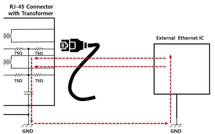
Figure 2 <common mode noise>
[Figure 2]
And 75 ohms behind the transformer is a resistor for common mode noise termination. As shown in Figure 2, since CHGND is connected to the outside, a loop is formed, which can cause noise induced in the cable as Tx and Rx signals to enter. This is called common mode noise.
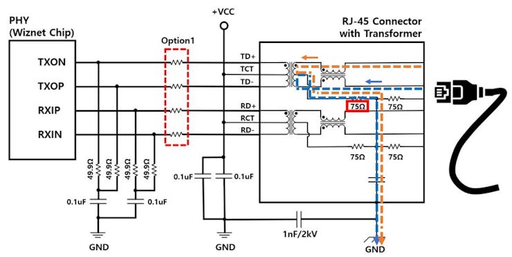
Figure 3 <75 ohm termination of common mode noise>
[Figure 3]
To remove this common mode noise, we attach a 75 ohm termination resistor, and this circuit is called a Bob-Smith circuit. Common mode noise coming in through the case is terminated through the center tap of the transformer.
(IEEE802.3 formally states that the common-mode impedance is 75 ohms for termination)
**There is still a lot of discussion about this circuit. (Example of interesting discussion)
Why is Bob Smith termination for Ethernet recommended if it's wrong?
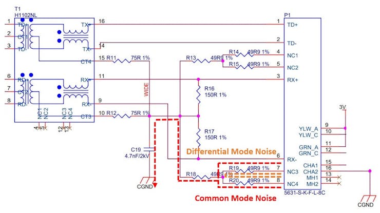
Figure 4 <Wiznet W5500 Reference Schematic>
[Figure 4]
If you look at 4, 5, 7, 8 in the figure above, you can see that there is a pair of 50 ohms in parallel, followed by one 50 ohm in series.
50|50+50 = 75 ohms for common mode termination and 100 ohm differential mode termination are designed.
Test progress
Now that the description of the circuit is over, the full-scale test proceeds.
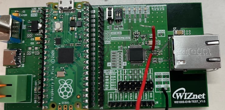
<W5100S-EVB-TEST-V1.0>
I connected the cables one by one to the Differential Line of the board. Waveform measurements were performed with a general oscilloscope.

<W5100S-EVB-TEST Circuit Schematic>

<Figure 5. RX+, RX- (left) versus GND / RX+ versus RX->
[Figure 5]
This is the result when the test is carried out according to the circuit above, which is the original circuit. Since W5100S is a PHY of Current Mode without internal bias, it has to catch the bias from the outside. This was set to 3.3V at the center tap of the transformer, so the voltage level was formed around 3.3V. And the differential voltage was formed with a peak to peak of about 2.1V.
It was confirmed that the waveform was normal and the operation worked well.
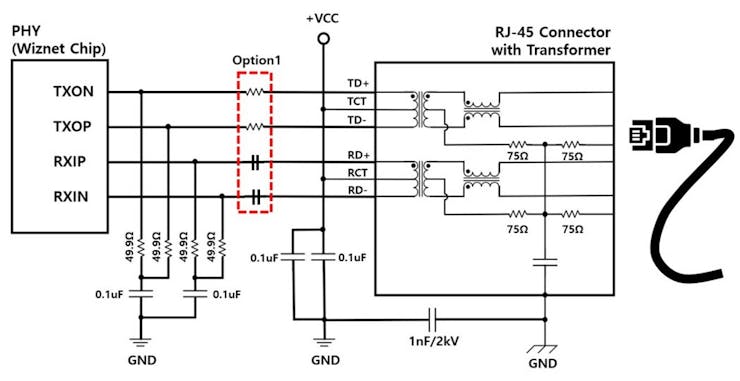
Figure 6 <Cap installed in place of damping resistor for EMC>
[Figure 6]
The EMC damping resistor of the Rx line was removed and a cap was installed. As a result, of course, the chip does not work because there is no DC bias. (Same for the Tx stage)

Figure 7 <Remove Cap and GND on Differential Mode Termination Resistor>
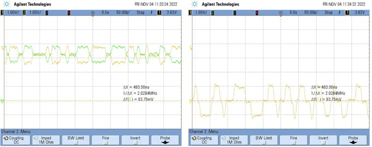
Figure 8 <RX+, RX- (left) versFigure 7. Remove Cap and GND on Differential Mode Termination Resistorus GND / RX+ versus RX->
[Figure 7]
I removed the capacitor and GND attached to the common mode termination resistor. Perhaps this part is for noise, so even if it is vulnerable to noise, it is likely to work.
[Figure 8]
Also, the operation works normally as in the existing circuit diagram.
* Then I wonder how it will work if the 50 ohm termination resistor is completely removed. In fact, there are data that have already been conducted for this test. i'll put it up.

Figure 9 <Connect VCC to Differential Mode Termination Resistor>
Figure 10 <RX+, RX- (left) versus GND / RX+ versus RX->
[Figure 9] [Figure 10]
This time, the power is connected to the terminating resistor. It works normally as above. Since the DC Bias is held by the transformer center tap, it all worked no matter how I connected power and GND to the terminating resistor.
*I don't know why the design connects to power and the design that connects to GND. Connecting to GND seems to be used as a filter. But what's the reason for tying it to power? Is it to smoothly flow current for Differential Mode in a circuit without DC Bias? If anyone knows the answer, please let me know.

<Figure 11. Connect VCC to Differential Mode Termination Resistor, remove +VCC to CT>

<Figure 12. RX+, RX- (left) versus GND / RX+ versus RX->
[Figure 11]
Connect +3.3V to the terminating resistor and remove the power from CT. The potential of CT becomes 0V. If there is no DC bias voltage in the chip, and the CT does not control the bias voltage, how will it work? The current circuit state is that the terminating resistor is also being used as a pull-up, but I was curious how the waveform would come out.
[Figure 12]
The bias voltage is not accurately set to +3.3V. Instead, Max Voltage is set to +3.3V Pull-up.
It was confirmed that the differential line waveform was captured well anyway. Anyway, even with this design, the chip reads the signal at the diff level, and the compliance test seems to pass normally. I wonder if this design is also a good design method.
(Diff Mode and Common Mode Termination are well designed, so EMC will be fine.)
**This is the part I am not familiar with. If anyone can let me know, I'd appreciate it.
In conclusion, in order to design a good Ethernet, the RJ-45 Datasheet must be carefully selected and designed according to the PHY Chip reference. There is no solution for EMC, and depending on the situation, if too much common-mode noise enters CHGND, it is also necessary to remove CHGND from the common-mode termination resistor of the Rx line. As such, many developers have their own know-how, and it seems to be a difficult topic as there are still many discussions.
Discussions
Become a Hackaday.io Member
Create an account to leave a comment. Already have an account? Log In.