 Ian Dunn
I've been a maker and an electronics enthusiast for my whole life. Designing custom PCB's is a specialty of mine. Somewhere along the way I realized that PCB's are a perfect medium for artistic works as well as electronic circuits. I have to give credit to Kelly Heaton for inspiring me to actually try it. I've created several circuit board art pieces and learned a lot along the way. I wrote this guide to share what I've learned about making art from printed circuit boards. I'll talk about making basic 2 dimensional PCB art, PCB art with electronic components, and how to make a PCB that is both beautiful and has electrical functionality. This guide is also relevant if your focus is PCB's that serve a primary function, but you also want them to look good.
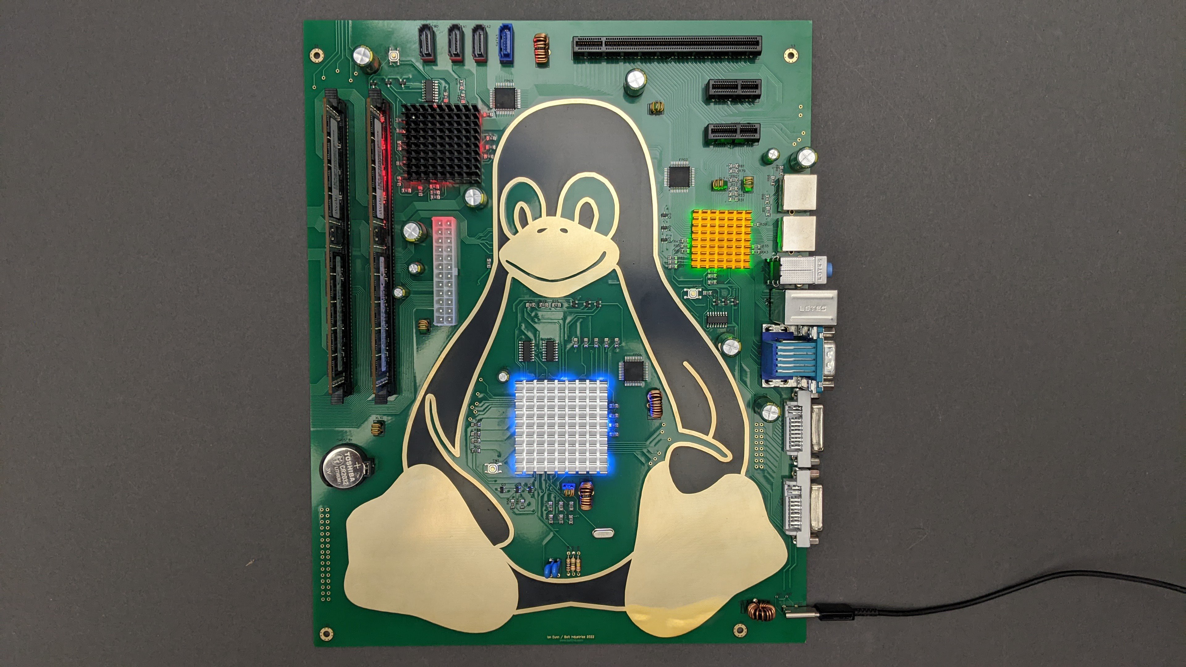
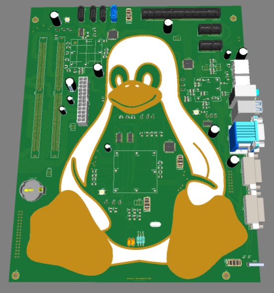
The Kickstarter campaign for the Tux Penguin ATX motherboard was unsuccessful. I had a lot of fun making it, and it will not be my last PCB art piece. Follow me here on Hackaday.io for more cool projects in the future. You can also visit my website, www.boltind.com where I have some PCB art for sale, and a lot of other cool open source stuff that's free for the taking.
It is a tradition of mine to write a Hackaday guide to accompany my Kickstarter projects, so here's everything you need to know to make your own circuit board art.
Solder Mask Colors and Copper Underneath
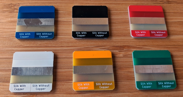
When it comes to PCB's, you're somewhat limited when it comes to colors. You can choose your solder mask color, and copper surface finish. Standard solder mask colors at most board houses are Green, Black, Red, White, Blue, yellow, and Purple. Black is the easiest to work with by far. It's usually a nice flat matte black color that looks really sharp. Some board houses seem to use a glossy black that is not nearly as nice. The other thing about black is that it['s opaque, so having copper underneath it won't really change it's appearance. All the same things are true about white. It is opaque, and white regardless of what is underneath it.
Pretty much any other solder mask color tends to be translucent, so you'll see the shiny copper traces or copper ground plane underneath it. This can be a problem with some colors. Green, Blue and Purple become washed out and dull if you add a copper ground plane underneath them. Smaller traces will be the same dull color, but it's not as noticeable on a small trace. It you want one of these colors, solder mask on top of the bare FR-4 without copper yields a much better color in most cases. The opposite is true of Yellow and red. I find that yellow looks a whole lot more Yellow with shiny copper underneath. Yellow on top of bare FR-4 is just plain ugly if you ask me. Red can go both ways. It's shiny and bright if placed on top of a copper ground plane. It's a little more muted if placed on top of bare FR-4, but still very red.
This is an image from an article on Hackaday.com that talks all about layers and solder mask colors. It does a great job of showing how each solder mask color looks. The link to the article is below.
Surface Finish
There are really only two options that I recommend for surface finish. ENIG (Electroless Nickel Emmersion Gold) or HASL (Hot Air Surface Leveling.) There are other options out there but they are a little exotic and a lot more expensive. I usually stick to ENIG. ENIG is a gold plated finish so it's more costly than HASL. HASL is just plain old silver colored solder in your choice of leaded or unleaded. There is not much of anything attractive about silvery gray solder, so ENIG is my go to choice. However I recommend always ordering the first board with HASL because no matter how confidant you are of your design, you will always want to change something when you actually get your board. Once you've got your board perfected with cheaper HASL, then go ahead and order it again in ENIG. This will save you money! If your design does not have any exposed copper, then go with lead free HASL.
I think it's safe to say that pretty much any solder mask color looks nice with gold finish. If you're going to pay for ENIG, you'll pay by the board size, not by the actual amount of gold finish. (Unless your entire board is covered in gold, they will probably ask for more money.) The catch is that some board houses will charge extra for ENIG on some colors other than Black and Green, so take this into account before you make a huge board that you want to order in Red with ENIG.
Neatly routed circuit board traces look good under solder mask, but they look awesome when they are exposed and gold plated! In Easy EDA the best way to do this is by selecting the trace, and pressing the "Expose Copper" button. This will add a solder mask layer identical to the trace. Any object in the solder mask layer will be treated as a hole in the solder mask in the final product. If you want to remove the solder mask on an object other than a trace, you can copy the object, paste it in the same place and change the layer to the solder mask. I'll elaborate more later on aligning these two layers.
Both of these boards below are ENIG. The traces on the board on the right do not have solder mask. It's easy to see that this the exposed traces look really cool.
Layers
In any EDA software, there's lots of layers to choose from. Most of them aren't needed, but the layers that are most useful for making PCB art are the copper, solder mask, and silkscreen. Copper is of course copper. Anywhere there is a copper trace in your design there will be copper on the finished product. The solder mask layer is backwards. Anywhere that you put an object in the solder mask layer, the solder mask will be removed on the board. If you put solder mask on top of copper, you will get bare copper with your finish of choice. If you place a solder mask object on it's own where it doesn't touch copper or a through hole then you'll get bare FR-4 substrate. Silkscreen is supposed to be used for lettering on the board. You can place silkscreen anywhere except bare copper. If you do place silkscreen on top of a solder pad or bare copper you will get no silkscreen.
Placing a copper ground plane, or at least some copper
I have found that every board needs to have al least one hole and at least one small bit of copper on both sides. You can get away without holes, but your board house will probably email you to tell you that the drill file in your Gerber is missing. If one or both sides are devoid of copper, they will probably tell you they have to charge you for an entire single sided FR-4 panel. An easy way to get around both of these problems is to simply add at least a single bit of copper to each side of the board, and at least one tiny drill hole or via.
Alignment of Layers
If you want bare gold plated copper, you have to be careful about the alignment between the copper layer and the solder mask layer. I think any board house will tell you that it's a good idea to make the solder mask layer a little bit bigger than the copper layer. I have found that this is not necessarily true. I think the thickness of the copper trace causes the silkscreen to pull into exactly the right place if you don't have a ground plane.
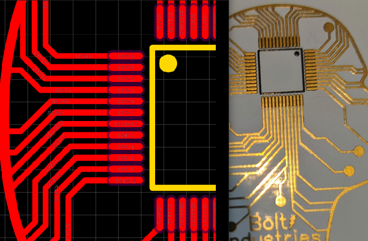
This image (left) is a close up of my company logo in EasyEDA. The red is the copper traces and the purple is the solder mask. Notice that I did not leave any extra slop in the solder mask layer over the traces. The solder mask layer does have some extra slop for the IC footprint. In the actual image on the right, you can see how this worked out. The alignment of the two layers is perfect! I regret not changing the solder mask layer size in the IC pads, because it meant that spot didn't get any solder mask. Those traces are .25mm wide.
Tracing Images with PCB Traces
Most if not all EDA software has a button to import images. This does not actually work very well! The edges of your shape tend to get blurred, and any sort of gradient will look horrible at best. A better way is to import the image you want into the document layer and trace it by hand with the wire tool. This is as time consuming as it sounds, but the result is worth the added effort. For best results, turn off snapping and set the routing angle setting to free angle. Zoom in really close and trace your image.
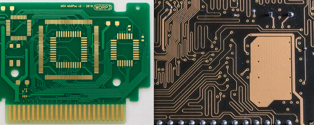
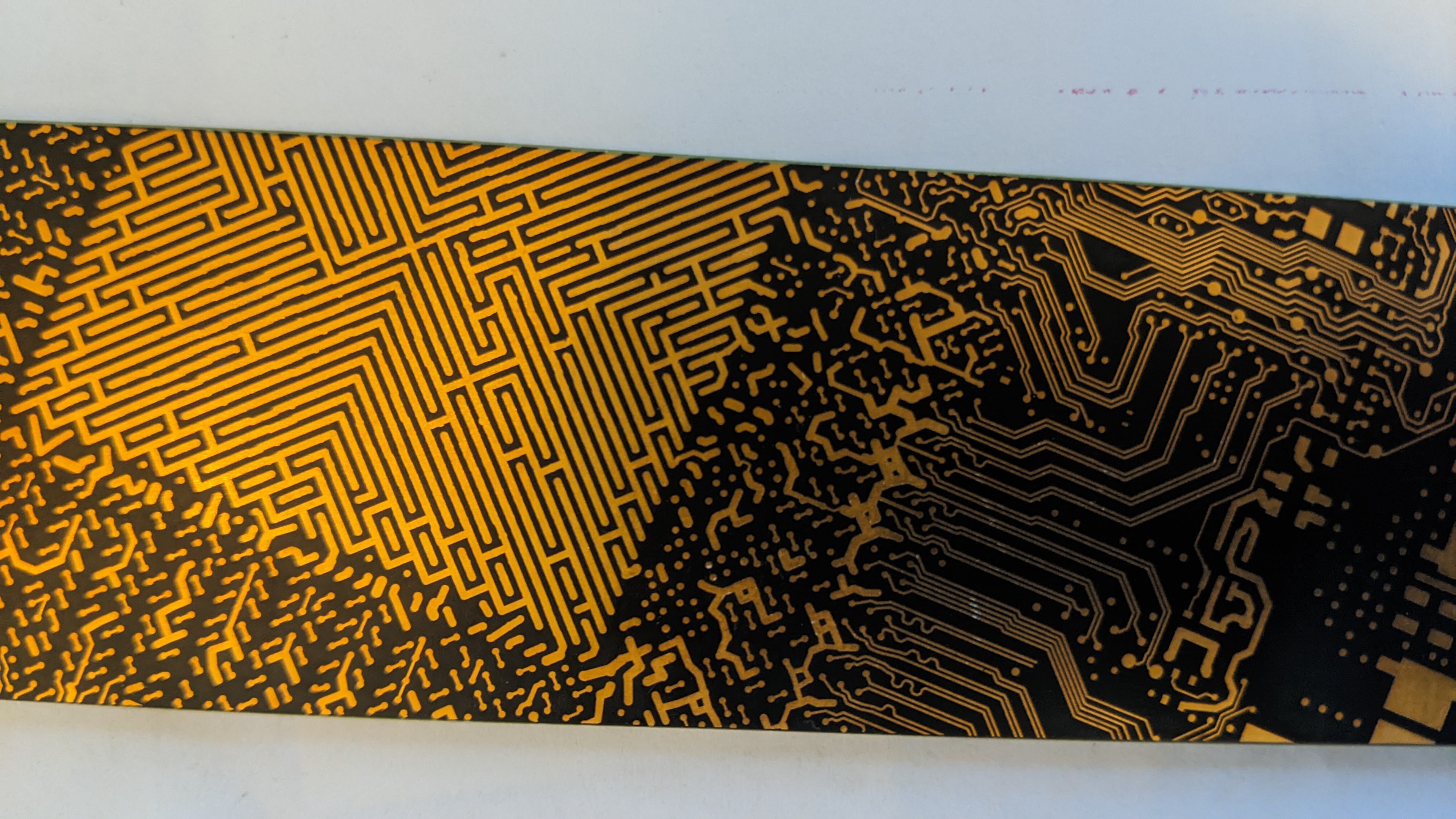
This Nvidia PCB ruler below is a great example. It's a beautiful ruler. One thing stands out to me about this design on the back: The traces toward the right are sharp and tidy. I think they were drawn separately in an EDA program. The big square thing on the left is grainy and wavy. I think it must be an image of a die taken with a microscope that got converted to a PNG with high contrast. I'll bet it got imported as a PNG into the bottom copper layer. You can see that the result is so-so and it stands out badly next to the nice sharp traces on the right.
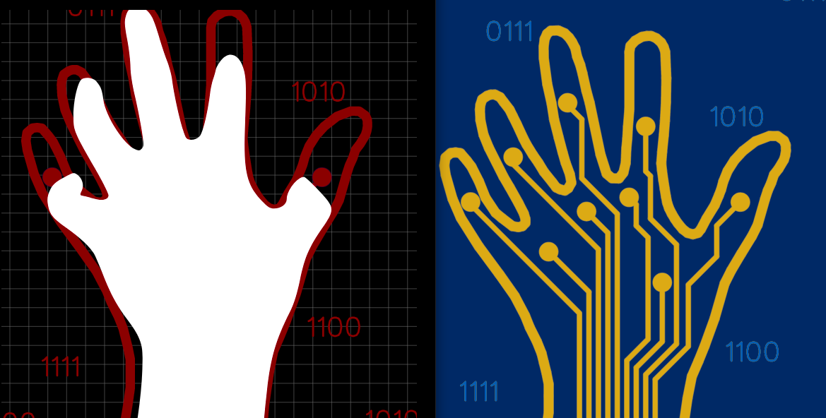
Below is a PCB art piece I'm currently working on. I needed a hand in it. I imported a PNG image of a hand, and you can see it in the white document layer on the left. It doesn't look very good! I traced it with a PCB trace and made some changes. You can see how it will look on the right. It's a lot better than the imported PNG.
Use both sides of the PCB
If your board does not have any components, then there's not any reason not to use the back of the board too and get your money's worth. It's not easy to draw a design backwards, so it's best to choose a design for the back that is symmetrical in a mirror image.
Adding Electrical Functionality
The ultimate challenge is to make a board that is both a work of art and has some electrical functionality. If you are going to go this route then I recommend getting your electrical circuit working perfectly first, then adding decorative elements. If you want to have non functional components or traces on the same board with functional things, it gets really tricky. You need to add all of the non functional components to the schematic with no connection flags on their pins. If you don't do this you will end up with hundreds of incomplete connection design rule violation errors that will cause the real design rule violations to get missed. It may be tempting to add the non functional components to the PCB directly, but they will be removed every time you change the schematic and update the PCB.
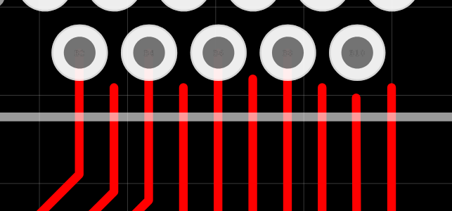
I highly recommend adding some decorative traces onto the PCB. This presents another problem when you check for design rule violations. You can't connect one component to another if it isn't connected in the schematic without causing a design rule violation. My work around is to make the decorative traces stop just short of the actual pad in a way that they are concealed under the component. The traces in the image below are only connected at one end or the other, not both. This allows them to be assigned to just one net.
Choosing Components
I recommend choosing components that have a 3d model connected to their footprint. This makes it easy to preview how your finished product will look. This works nicely with Easy EDA's 3d preview function.
Just about every electrical component made in the USSR is beautiful. For example, they were really good at making IC's in unusual packages with gold leads that are works of art by themselves. There's lots of cool USSR components on eBay from a few sellers in Ukraine that have a wide variety. Surplus stores are another good place to go. Vintage CPU's are hard to go wrong with. They can be found on eBay as well. I've found a few modern components that I like too. High wattage carbon film resistors resistors and small axial through hole inductors usually have a lot of good colors. I like dipped tantalum capacitors and 3KV (or higher) ceramic disk capacitors, both tend to be a beautiful blue color. Surface mount LED's are easy to hide under something else to add a splash of light. You can't go wrong with doughnut shaped inductors. Regular through hole electrolytic capacitors can be found in different colors that look nice. Plane old black diodes are a good way to add black and they come in all sizes big and small. Heat sinks are another good one. Something that I want to try is rear mounted SMT LED's to back light a translucent PCB.
Component footprints without the actual component are a good way to go too. I like having an assortment of PCB rulers with component footprints in front of me to reference for this. I also have a set of Cheat Cards that are loaded with component footprints.
We've all seen electrolytic capacitors, inductors, and 14 pin DIP's so I won't bother adding pictures of those. Here are a few pictures of components that stand out to me as good choices for art.
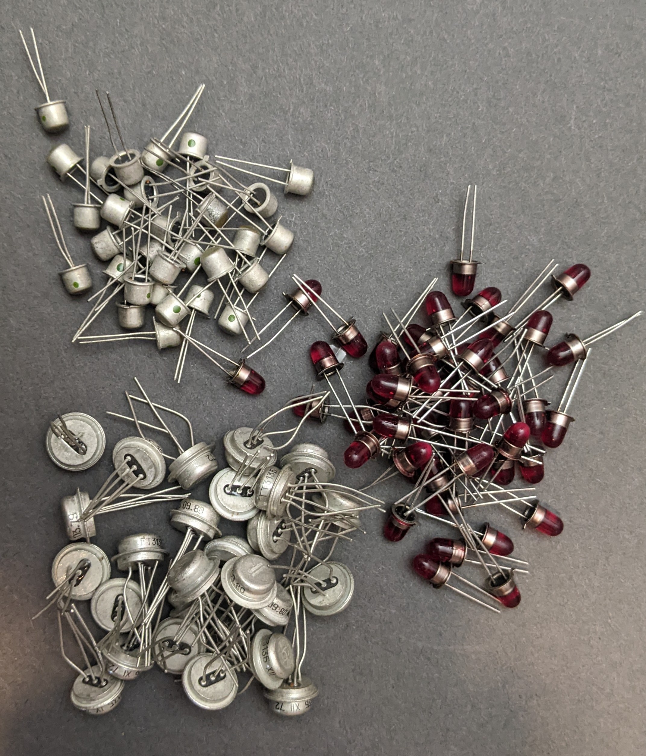
Just about any parts made in the USSR are beautiful! These are green and red LED's and some PNP transistors.
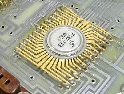
This is a great example of the Beautiful IC's that came from the USSR.
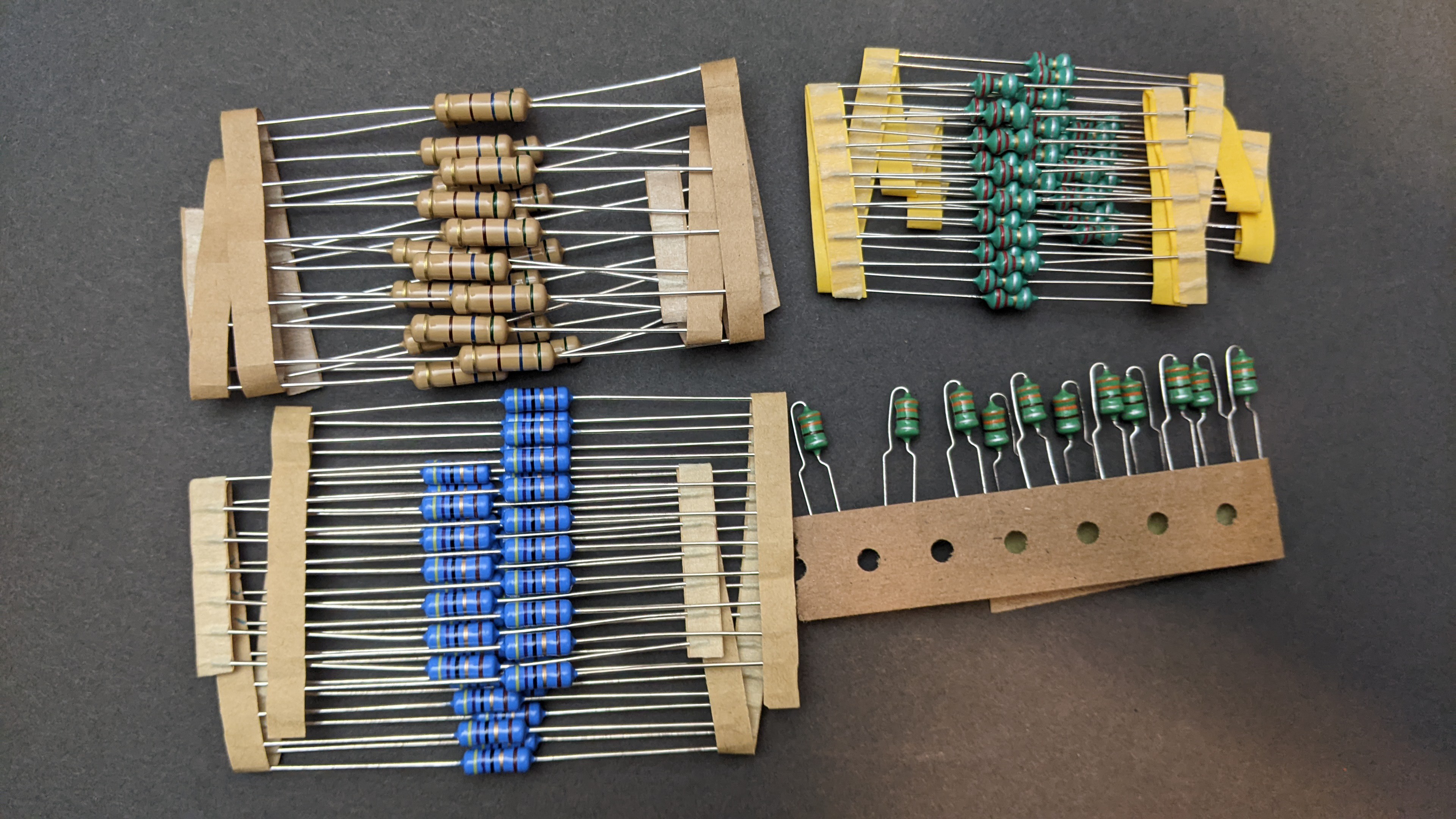
Really big carbon film resistors, (brown) Metal oxide resistors, (blue) and two varieties of small inductors (green.)
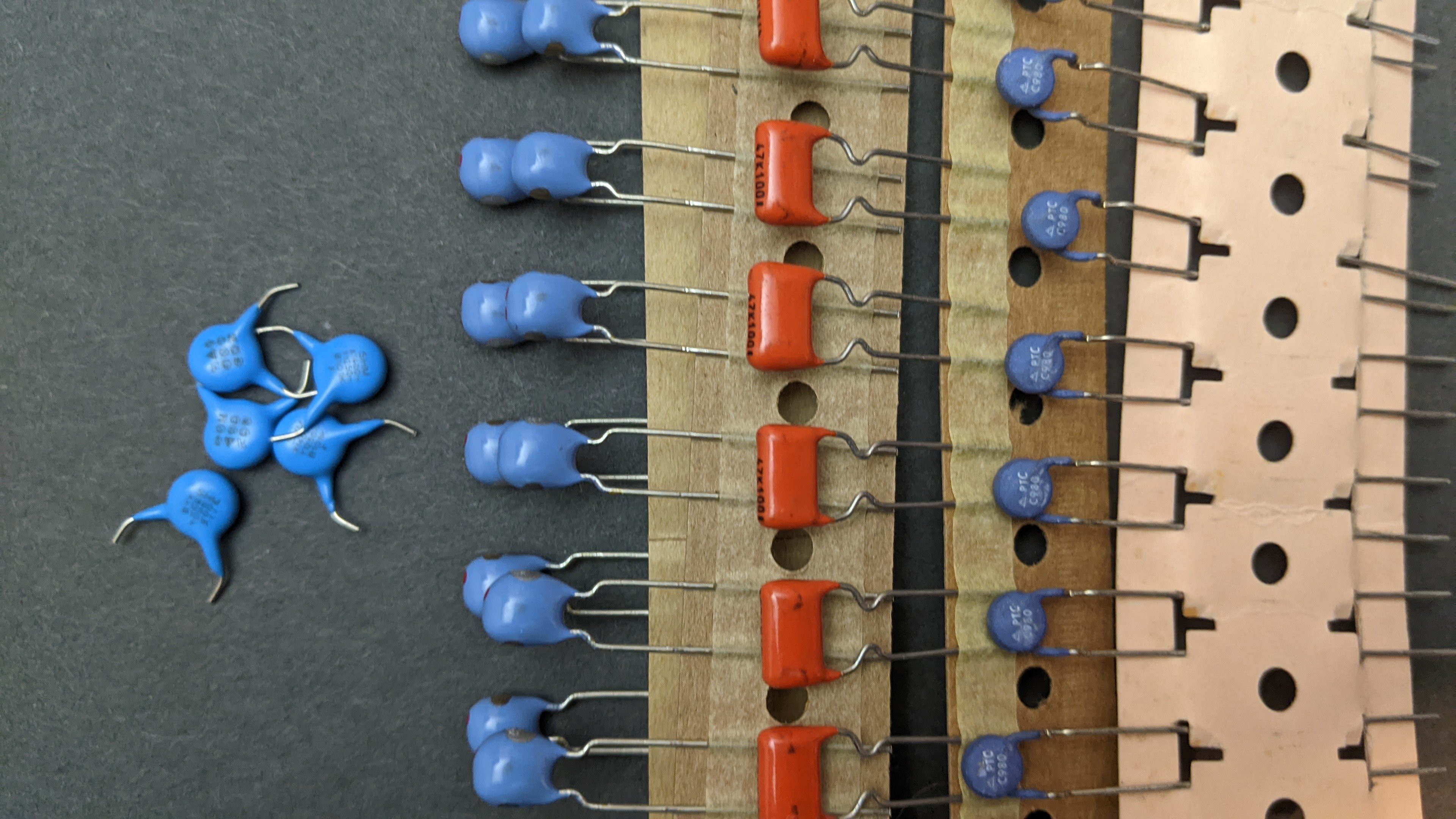
These are some capacitors that I picked up at a surplus store. Through hole tantalum caps (in the paper holder on the left) are hard to find, but they sure do look cool! The others are just good examples of nice looking ceramic caps.
How will it actually look in the end?
I highly recommend using the rendering functions in your EDA to preview how your board will look. Print your rendering out on paper and study it this way, I guarantee you will find something to change.
What board house to use?
This is not an endorsement or sponsored advertisement for any PCB fab house. I'll just talk briefly about a few board houses that I like and why.
JLCPCB is good for almost any board that does not require assembly. They do a great job almost all of the time. For a simple 2 layer board, their prices really can't be beat and they do a great job. They are really fast and constant. If you need any components soldered onto your board, I find that they have too much annoying red tape for their assembly service to be useful. They will only allow you to source certain components from certain vendors among other things.
PCB Way is about twice the price of JLCPCB, but they have a lot more color choices and they will assemble your boards with any components from anywhere in any quantity without any silly red tape. I have gotten scratched or damaged PCB's from them, but they will always fix their mistakes unlike JLCPCB. They have a great assortment of solder mask and silkscreen colors, and the best part is that you can choose your solder mask and silkscreen colors separately!
Thanks for reading along. I hope I've inspired you to try making some PCB art of your own.
Ian