 zpekic
EMZ1001A has 51 different instructions (52 with BRK) if counted by assembly name mnemonic. All 256 op-codes are used, but with 6-bit address for JMP and JMS, this means each of these takes 64 op-codes, and all the other instructions 128. State machine with 52 distinct states would be complex and slow, but after analyzing the instruction set, collapsing this number is possible:
- All ALU instructions of A = A op X pattern can be grouped together
- All SKIPs are the same, just vary the source to be loaded into ir_skp flip-flop (only exception is SOS which also resets the 1s counter)
- Setting / clearing of TFx flags is same operation, the new value can be picked up from instruction register (ir_current) LSB
With the above optimizations, 32 different operations are sufficient (5 control bits)
If we split ALU operations that update carry (mr_cy) and accumulator (mr_a) registers, we see that they are only ADC, XOR and AND operations with A, RAM, Immediate (LSN of ir_current) as inputs, but not all combinations of these are needed. 8 are enough to select the required operation (3 control bits).
Finally, analyzing the SKP instructions, we see that 16 sources are sufficient (4 control bits).
With 4 + 3 + 5 control bits, any instruction can be uniquely identified, and each of the 3 main control units driven independently: ALU, SKIP and the register update process.
Obviously, a lookup-table is needed to map from instruction op-code to the corresponding control signals. This would be a 256*12 ROM, but because JMS and JMP would be repeat 64-times, splitting the instruction space to 4*64 with a 4 to 1 MUX tied to instruction registed bits 7 and 6 allows cutting this memory requirement in half:
-- instruction decode (256 op-codes split into 4*64 blocks)
with ir_current(7 downto 6) select pla <=
    pla_00(to_integer(unsigned(ir_current(5 downto 0)))) when "00", -- NOP to LAM
    pla_01(to_integer(unsigned(ir_current(5 downto 0)))) when "01", -- LBZ to LAI
    skp_0 & alu_nop & opr_jms when "10",      -- JMS
    skp_0 & alu_nop & opr_jmp when others;    -- JMP
We see how JMS and JMP are defined as a concatenation of 3 control fields, pla_00 and pla_01 hold these for all the other instructions. "pla" (programmable logic array) is a mis-nomer here because these are simple ROMs, no AND/NOT/OR logic array, but could be implemented in that way.
The MUX above is central piece of the instruction decode logic:
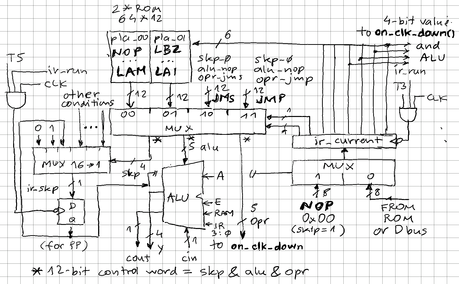
Resulting 12-bit control word is drives most of the processor internals:
-- instruction decode
signal pla: std_logic_vector(11 downto 0);
alias skp: std_logic_vector(3 downto 0) is pla(11 downto 8);
alias alu: std_logic_vector(2 downto 0) is pla(7 downto 5);
alias opr: std_logic_vector(4 downto 0) is pla(4 downto 0);
skp - skip
skp is driving a MUX that selects the 1-bit flag or value to load into ir_skp register, which will be checked to either execute the instruction or mask it with 0x00 to become a NOP (which has same effect as skipping). Note the value for PP (prepare page) - skip bit is a pass-through so that is 1 PP is skipped, any subsequent is skipped too. This allows conditional JMP/JMS to any location, not just on current page.
-- select source for updated skip flag (16 to 1 mux)
with skp select y_skp <=
--		'0' 	when skp_0,	-- never skip next instruction
		'1' 	when skp_1,	-- always skip next instruction
		ir_sec  when skp_sec,
		bl_equals_e when skp_ble,
		(not mr_cy) when skp_cy0,
		(not y_alu(5)) when skp_cout,
		a_equals_m when skp_am,
		(not bit_is_1) when skp_bit,
		bl_is_15 when skp_blf,
		bl_is_0 when skp_bl0,
		not(ik(3) or ik(2) or ik(1) or ik(0)) when skp_ik,	-- at least 1 zero detected in I or K after masking
		ir_skp when skp_skp,	-- do not change skip flag, pass it to next instruction
		mr_f1 when skp_f1,
		mr_f2 when skp_f2,
		'0' when others;	-- no skip by default
alu - arithmetic logic unit
ALU is also implemented as a MUX. There are several sources for operations (A, RAM, immediate from instruction register) and few operations (AND, XOR, ADD with and without carry) but not all combinations are present, so 3-bit selection is sufficient:
-- terribly non-optimal 6-bit wide ALU (carry-in + 4 bits + carry-out)
with alu select y_alu <=
		mr_cy & (mr_a xor X"F") & '0' 	when alu_cma,
		mr_cy & (mr_a and ram) & '0' 	when alu_and,
		mr_cy & (mr_a xor ram) & '0' 	when alu_xor,
		std_logic_vector(unsigned('0' & mr_a & mr_cy) + unsigned('0' & ram & mr_cy)) 		when alu_adcs,
		std_logic_vector(unsigned('0' & mr_a & '0') + unsigned('0' & ir_current(3 downto 0) & '0')) 	when alu_adis,
		mr_cy & std_logic_vector(unsigned(mr_a & '0') + unsigned(ram & '0')) 							when alu_add,
		not(ir_current(0)) & mr_a & '0'	when alu_cry,	-- passthrough to set carry flag
		mr_cy & mr_a & '0' 					when others;
The idea is that all updated to carry (mr_cy) and accumulator (mr_a) go through ALU, even if just as a pass-through, that way process operation is very simple:
...
        when opr_alu =>	-- ADD, ADCS, ADIS, AND, XOR, CMA, STC, RSC
	    -- ADIS must generate carry out for skip, but should not store it!
	    if (ir_current(7 downto 4) = "0101") then
		mr_cy <= mr_cy;
	    else
		mr_cy <= y_alu(5);
	    end if;
	    mr_a <= y_alu(4 downto 1);
....
opr - register update operation
Finally, the 1 out of 32 operation IDs are consumed in a switch statement within the main process that updates the processor registers. It is up to the VHDL compiler to recognize the process as a state machine and encode these states for fastest decoding based on the settings and nature of the FPGA. The most interesting operations are for XC, XCD, XCI instructions that simultaneously update RAM plus 2 or 3 other registers at the same moment, which is pretty remarkable for a 4-bit CPU.
...

    when opr_xc0 =>	-- XC
	mr_ram(to_integer(unsigned(ram_addr))) <= mr_a;
	mr_a <= ram;
	mr_bu <= bu_xor;
    when opr_xci =>	-- XCI
        mr_ram(to_integer(unsigned(ram_addr))) <= mr_a;
	mr_a <= ram;
	mr_bu <= bu_xor;
	mr_bl <= bl_inc;
    when opr_xcd =>	-- XCD
	mr_ram(to_integer(unsigned(ram_addr))) <= mr_a;
        mr_a <= ram;
	mr_bu <= bu_xor;
	mr_bl <= bl_dec;
...
Note that there is no "ALU" behind incrementing / decrementing BU (mr_bu) or XOR'ing BL (mr_bl) registers - with known register values and instruction register lower 2 bits, the new values can be looked up in a table and result assigned as new value of BL, BU.
Discussions
Become a Hackaday.io Member
Create an account to leave a comment. Already have an account? Log In.