0%
0%
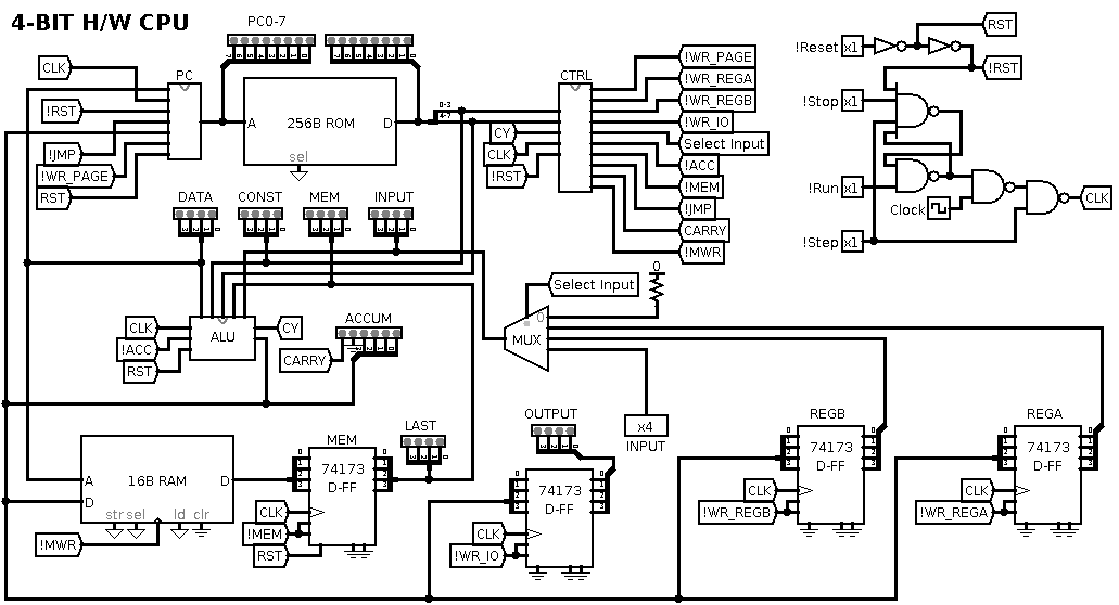
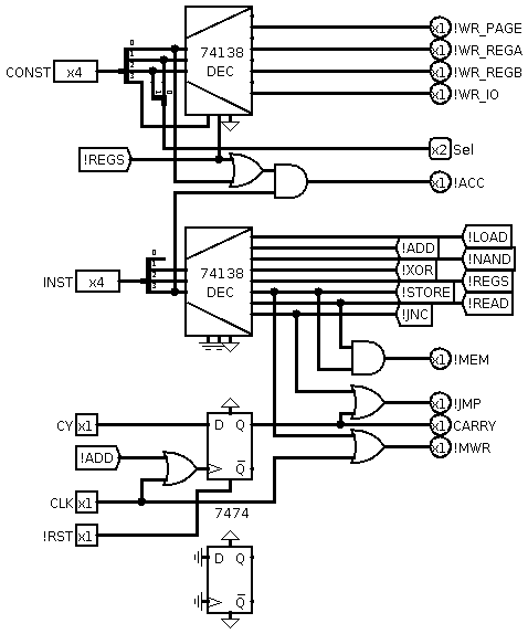
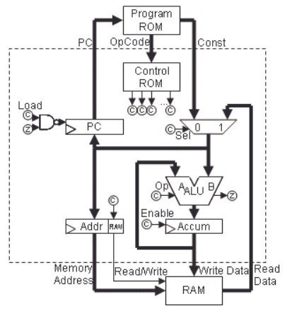
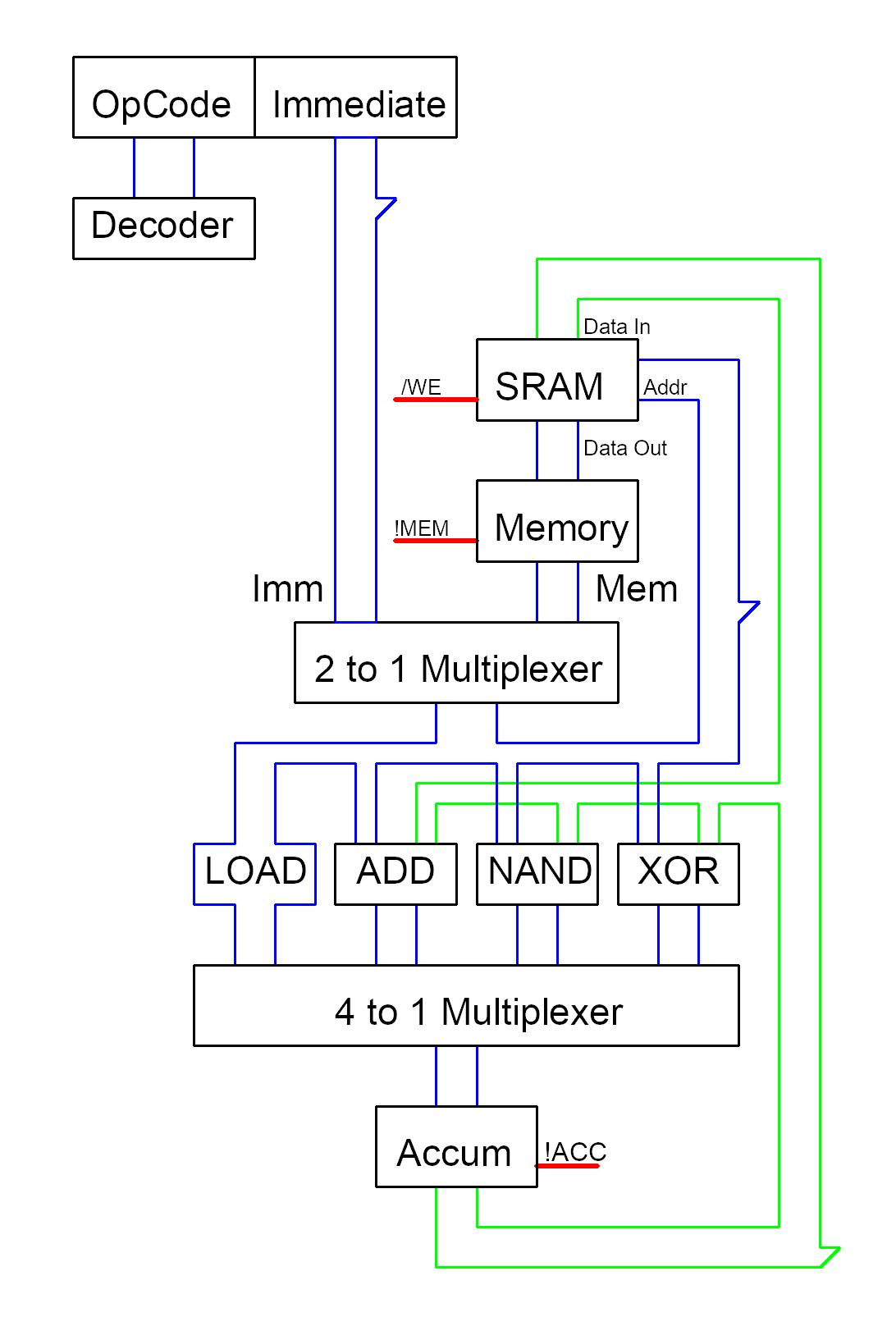
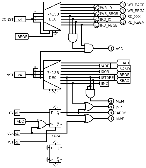
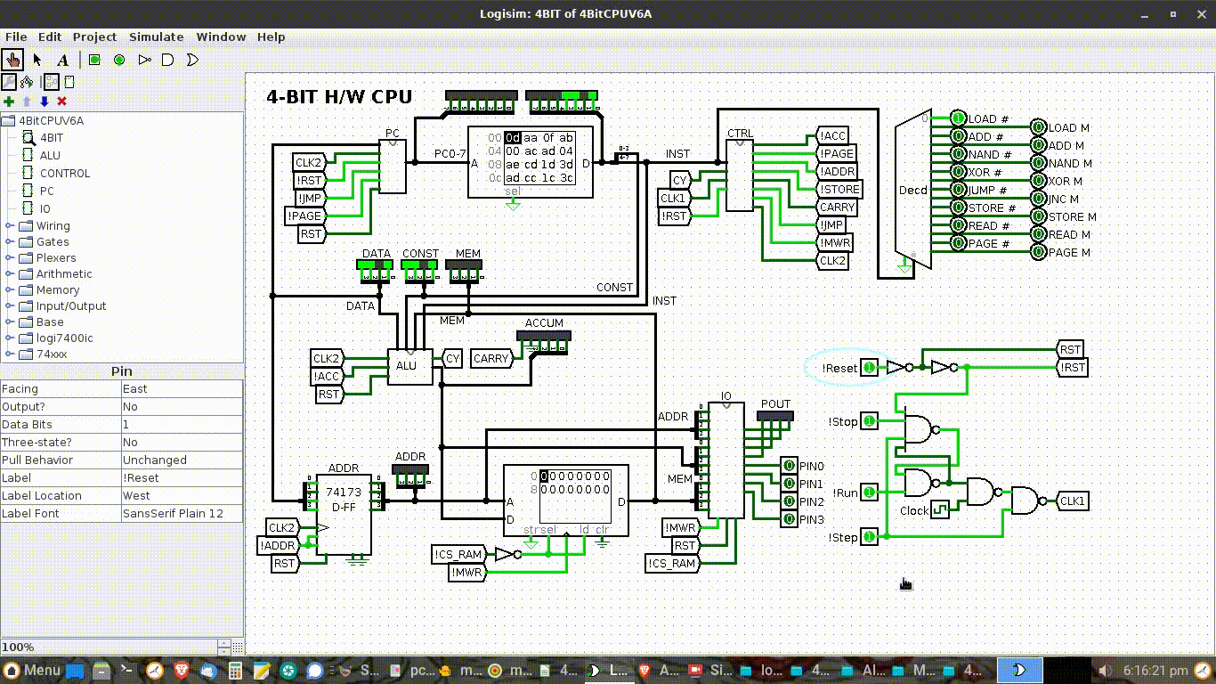
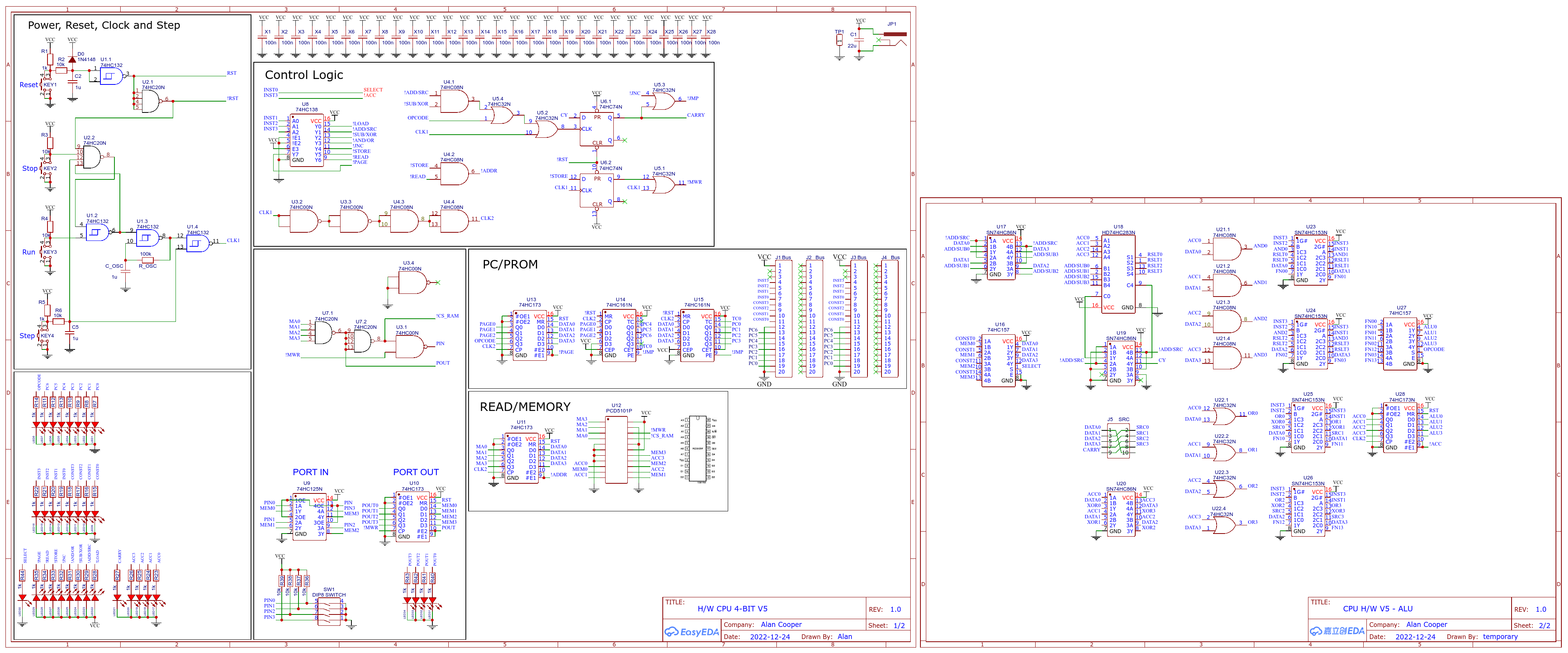
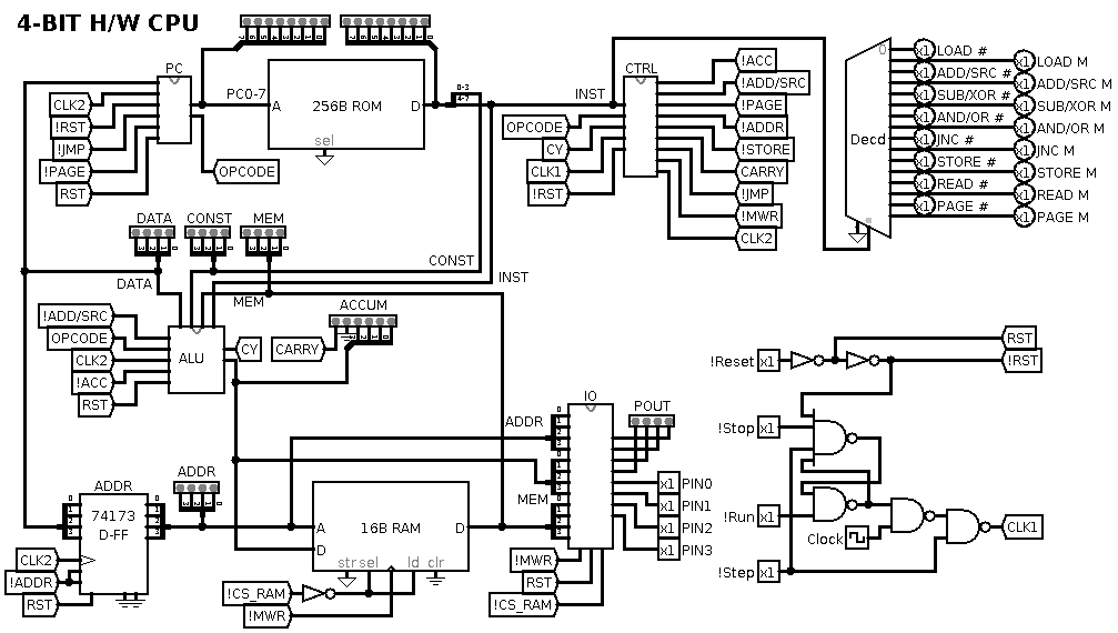
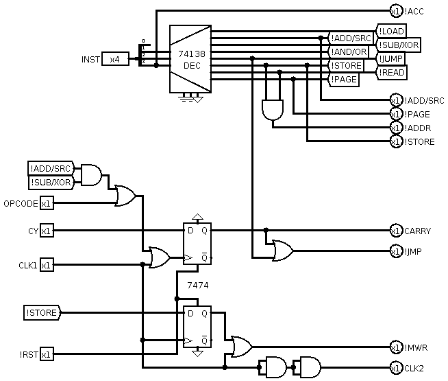
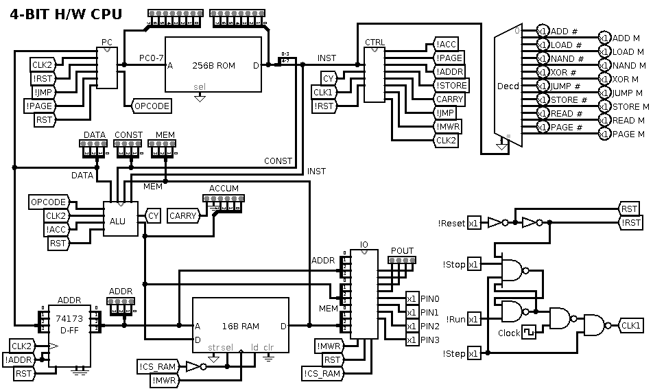
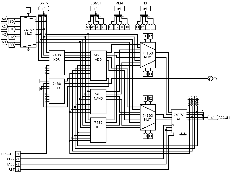
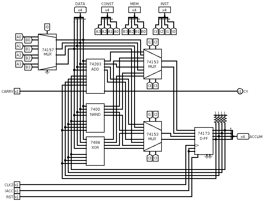
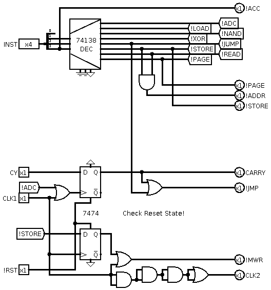
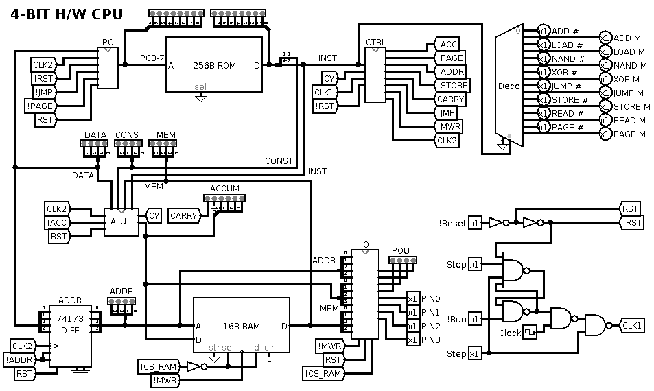
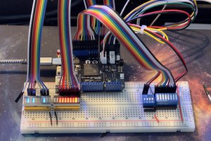
Hardware Controlled 4 bit CPU
A hardware controlled 4 bit CPU based on lessons learnt from the TD4 and the CHUMP CPUs
 agp.cooper
Become a Hackaday.io member
Already have an account? Log in.
Just one more thing
To make the experience fit your profile, pick a username and tell us what interests you.
Pick an awesome username
hackaday.io/
Your profile's URL: hackaday.io/username. Max 25 alphanumeric characters.
Pick a few interests
Projects that share your interests
People that share your interests


 Tom
Tom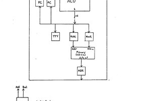
 kaimac
 Tim
Tim
I am impressed with your project. can you tell me if I can use this for my
https://www.fitnessrap.com/product/helimix-2-0-vortex-blender-shaker-bottle/