 Eric Hertz
UPDATE: Re: Project "Reveal" and realistic goals in the following few paragraphs...
------
This should've been two separate project-logs... The "secret-reveal" was supposed to be a minor bit merely as lead-up to the current state-of-things (interfacing with the bus).
-------
In case you haven't figured out "the secret" of this project... the idea is to use an AVR to emulate an 8088 *in circuit*... To pop out the original 8088 in my (finally-functioning) PC/XT clone, and pop-in my AVR, and see what the blasted thing's capable of.
A key observation, here, is that AVRs run at roughly 1 instruction per clock-cycle, while 8088's can take *dozens* of clock-cycles for a single instruction. I read somewhere that the 4.7MHz 8088 in a PC/XT runs at something like 500*K*IPS. Whereas, an AVR running at 20MHz would run at something like 20MIPS! FOURTY TIMES as many instructions-per-second!
(albeit, simpler instructions, only 8-bit, and I imagine much of the limitation of an 8088 is the fact it's got to fetch instructions from external memory at a rate of 1/4 Byte per clock-cycle... which of course an AVR wouldn't be immune to, either.)
Anyways, I think it's plausible an AVR could emulate an 8088 *chip* at comparable speed to the original CPU. (Yahknow, as in, taking minutes, rather than hours, to boot DOS). Maybe even play BlockOut! (3D Tetris).
But those are *Long Term* goals, and it's entirely likely I'll lose steam before even implementing the majority of the instruction-set. For now, I intend to pull out the BIOS ROM, and replace it with a custom "program" using an *extremely* reduced instruction-set...
First goal is to output "Hello World" via the RS-232 port... I think that wouldn't take much more than a "jump" and a bunch of "out"s... so should be doable, even by the likes of me.
...And, maybe, just maybe, I could fit that and the reduced "emulator" in less than 1K of total program-memory on the two systems (and not making use of other ROM sources such as LUTs for character-drawing on the CGA card)... A bit ridiculous, there's only a few days left for the https://hackaday.io/contest/18215-the-1kb-challenge, and I haven't even decided on which AVR to use....
(Regardless of the contest, it's an interesting challenge to try to keep this as compact as possible. You can probably see from the previous logs I've already been trying to figure out how to minimize the code-space requirements for *parsing* instructions... *executing* them is still a *long* ways off ;)
------------
I was planning to use my trusty Atmega8515, since I've a few in stock...
I think it has *exactly* as many I/O pins as I need...
But... it gets complicated because:
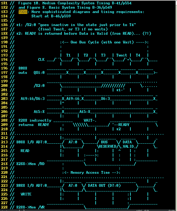
The 8088 clock runs at 4.77MHz, this is derived from a crystal running at
14.318MHz (divided by 3), but that signal's not available at the processor.
8-bit AVR clocks generally max-out around 16-20MHz (but can be overclocked
a little, and sometimes even quite a bit).
The 8515 is rated for 16MHz. And, worse for this project, its internal (and
*calibratable*) clock is limited to somewhere around 8MHz.
So, let's say I could bump that up to 4.77*2=9.54MHz via the OSCCAL
(oscillator calibration) register... That means I'd only be able to execute
*two* instructions between each of the 8088's clock-cycles.
And, seeing as how the AVR is only an 8-bit processor, there's no way it'd
come close to the 8088's bus-timing, what with needing to write 20 bits in
a single 8088 cycle (A19:16, A15:8, A7:0, at the beginning of T1).
In my initial estimates, I was planning on having 4 AVR clock-cycles for
every 8088 clock-cycle. That's not far-fetched... 19.09MHz. (Again,
most AVRs these days are rated for 20MHz, and the 8515-16MHz could probably
handle 19MHz). Doable, but I'd need an external clock for the 8515, and
somehow would need to calibrate it to closely-match the 8088's (which, too,
can be adjusted via a variable-capacitor).
-------------
I also have a couple ATmega644's, MUCH more sophisticated, in general, than the 8515, (mostly due to increased memory, but also a few additional instructions) but these guys have a similar internal clock, and fewer I/O pins...
-------------
I have a bunch of ATtiny861's... These guys have an internal R/C
(calibratable) oscillator that runs at ~8MHz, as well.
BUT, it can be bumped-up to a higher system-frequency with the internal PLL.
So, I've some vague theory that if I take the 8088's 4.77MHz clock and feed
it into a Timer Input-Capture pin... I might just be able to create ....
Can the PLL be configured to sync with an external clock?
(Update: NOPE)
The thought is... using the Timer's Input-Capture pin, I could write a
little routine that runs at Power-Up, that adjusts OSCCAL to match the 8088's
clock, except at a higher multiple... e.g. 4x (19.1MHz), or maybe even 5x
(23.9MHz).
And then... I'd be able to execute 4 or 5 AVR instructions per every 8088
clock-cycle... which should be *just* enough to handle writing *all the*
address-bytes in a single bus-clock. (NOT within the 8088 timing-specs of
something like 100ns from the clock-edge to the 20-bit address-output, but
we'll see where that goes. I should probably look into the 8288 and other
"slave"-devices' expectations, since they're what really matter).
.......
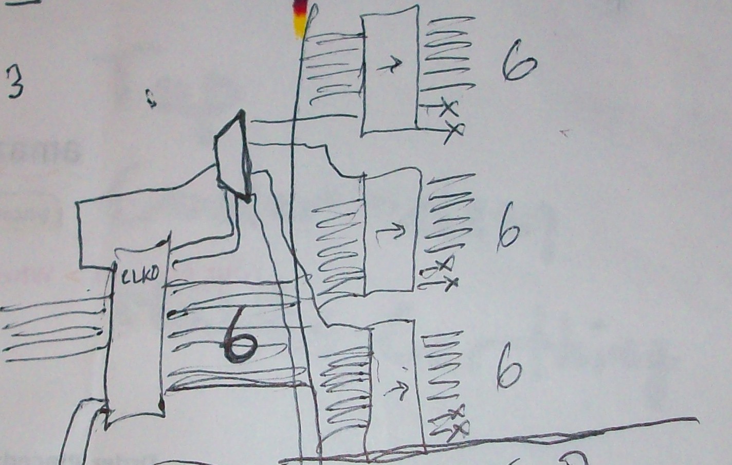
Thing is, the Tiny861 only has TWO 8-bit ports, and no other pins for I/O.
(Trying to do the work of a 40pin 16-bit CPU with a 20-pin 8-bit microcontroller!)
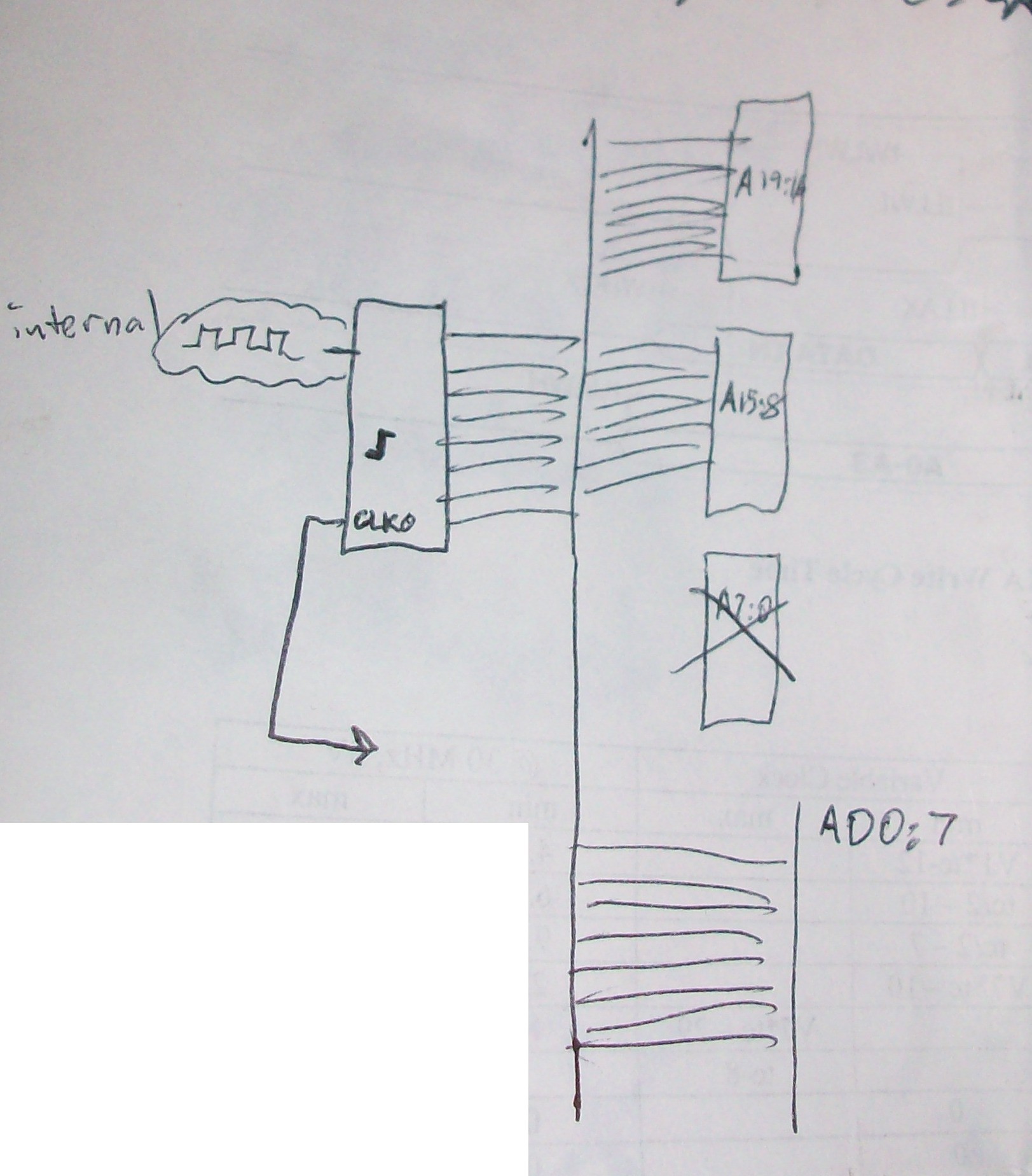
You can see from the above diagram, for bus-interfacing alone, I need
18 outputs (A19:16, A15:8, /S2:0, QS1:0 and /RD) *as well as* 8
I/Os (AD7:0) (which I'll come back to later).
-----------
Say for those 18 outputs I use 3 8-bit latches such as the 74AC574's in my
collection. Those latch on the rising-edge of their clock-input.
Alrighty... Something like:
Here's a single bit routed to two latches:
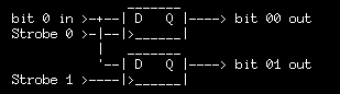
This would take 3 AVR clock-cycles to write each byte-wide latch. (Write-Data to Latch-Inputs, Strobe-high, Strobe-Low).
Short of pins, the strobe inputs could be reduced via demuxing:
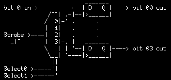
Now I can handle four bytes with only 3 additional GPIOs.
This might take an additional AVR clock-cycle to write a byte-wide latch. (Select, Write-Data, Strobe-high, Strobe-Low).
But we got here because this system's already too slow! It was already too slow when I could write each byte-wide port on the original 8515 with a single instruction! (Three address-bytes, three ports, three AVR-instructions, needed to fit within one 8088 bus-clock).
So, these muxing-schemes would make the system *even slower*. No good.
---------The Tiny861 has an optional clock-output that matches its internal clock...
And Tiny861 outputs are toggled on the rising-edge of the internal
clock. What if I use that output-clock as the "strobe" for my latches?
Then I wouldn't need a GPIO to toggle twice for each latch operation, reducing the latch-write-instruction-count to 2 (select, write).
(This may introduce a glitch between select/write, but that can be dealt-with).
And I reduce the GPIO-usage by one pin.
But, we'd have the same problem... I'd first have to select which latch,
then write the 8-bits of data... 6 instructions to write three bytes.
(select, write, repeat, repeat), and still only 4, maybe 5 instructions can fit within an 8088 bus-clock.
-------------------
Ignoring AD7:0, for now, I need 18 outputs to transition during a single bus-clock...
And 18/3 just happens to be 6...
So, if I only used 6 of the 8 latches in each chip, and only wrote 6 bits
each time, I'd have two remaining pins on the AVR's 8-bit port.
Two pins which could be fed into the select-inputs of a 1-in-4-out demux,
for instance! (Random luck, here!)
AND, Importantly, those two pins, on the same port, would be written at the same time as the 6 address-bits-to-be-latched, so only *one* instruction must be executed to both *select* a latch *and write* data to it!

Now, I haven't *fully* wrapped my head around this, yet... It might be
necessary to insert some delays between the AVR's Clock-Output and the
demux's input, such that the data arrives at the latches' inputs *just
before* the clock-output reaches the selected latch's clock-input. But I
think that can be handled with little more than a few gates inserted for
the sake of adding a delay. OR, maybe... inserting a (fast) inverter
inbetween, so the latches' inputs are loaded with data on the rising-edge
of the AVR clock, but the latches are clocked on the following (inverted)
falling-edge of the AVR-clock.
Should be doable.
AND, amazingly, will take *exactly* the same number of AVR
instruction-cycles to write these three external latches as it would've to write
3 dedicated I/O ports (on a chip which has that many).
(Of course, a little preprocessing would have to be done, to merge the data
and select info. But, the actual writing of the three latches will take
exactly 3 instruction-cycles. And that's what's important, here... that the
changes all occur within a single 8088 bus cycle).
=====================
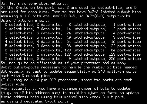
I wrote a program to calculate the possibilities for future-endeavors:
------------------
TODOs:
For the I/O byte (AD7:0), I'll use the fourth output from the demux. I've some ideas regarding that, including some that've been well-thought-out in #sdramThingZero - 133MS/s 32-bit Logic Analyzer, making use of resistors as data-paths (and virtual "open-circuits") without necessitating additional Output-Enable or Direction signals (which would have to be driven by GPIOs). I'll come back to that later.
So, assuming I run my AVR (Tiny861?) at 4x the 8088's bus-clock, we'll *just* fit in all the necessary transitions. With QS1:0 changing midway, that might add a 5th transition (5x clock is pushing it, but plausible).
The 8088 timing specifications show those transitions happening within a very short time-period... E.G. ALL the address-bits (20!) are supposed to be written within 100ns of the bus-clock's edge. Again, doubtful an 8-bit AVR could handle all that in 100ns. But I've some ideas for how to make it work if it really needs to be *that* precise. Good thing I ordered so many 74AC574's!
Discussions
Become a Hackaday.io Member
Create an account to leave a comment. Already have an account? Log In.
@esot.eric
I think I understand what you are saying, this topic is complicated and can increase blood pressure easily. Even good-intended comments can look like unneeded mentoring.
Oh, we are getting rather off-topic. Though this could be nice "beer debate" - let me know if you happen to walk around ;-)
Are you sure? yes | no
Indeed, there's a lot of hand-waiving in this field, and a lot of folks who hand-wave prematurely.
My original comment regarding 'ACs to Ted was a head-nod for informing me (in another thread somewhere I've long since lost track of) of something I hadn't yet known about: 'ACs' issues with ground-bounce.
Are you sure? yes | no
Back on topic, I re-found these two application notes about 74AC logic ground bounce and terminations while researching a recent project. I meant to provide links in our previous discussion, but couldn't find them at the time.
https://www.fairchildsemi.com/application-notes/AN/AN-610.pdf
https://www.fairchildsemi.com/application-notes/AN/AN-640.pdf
Are you sure? yes | no
Thanks @Ted Yapo for those links!
The first looks to be about reflections, termination, etc... which is great information for all fast-logic ('AC, or otherwise, and even fiberoptics). I recall spending quite a bit of time in the ol' college courses on the matter, and an entire summer doing simulations of these things for DDR-RAM and gigabit-fiber in an internship.
The second looks to be about Ground-Bounce, which was something I don't recall from those courses or elsewhere, and seems to be especially a concern with the 'AC series, as many newer (and even faster/higher-drive-strength) series seem to claim many of those concerns have been minimized. However, it still seems like it'd be a concern with fast-logic besides the 'AC series, especially when driving large loads, or when switching many outputs simultaneously. That datasheet ends with some "Design Rules" which amount to slightly-more-sophisticated versions of "It Works" ;)
Are you sure? yes | no
8086 emulation is a thing I started for something like... half a dozen times? I wish you best luck with this project, achieving at least one fifth of real 8086 performance would be great success!
Are you sure? yes | no
LOL that's a little disheartening, and part of the reason I hesitated to reveal the secret. Dare I, someone who just looked at x86 assembly for the first time less than a month ago, ask why you've "started" (and presumably not finished) so many times?
Are you sure? yes | no
Don't know why, but 8086 architecture and instruction set makes me a bit sick. It feels so unclean, hacked-together and rough. I always promised myself to behave "profesionally", to not to look at it and just write an emulator, but I couldn't resist.
I wanted to make 8086 (I use 8086 as generic term for 8088 too, as you probably noticed) emulator to emulate IBM XT machine in some MCU, like PIC32MZ - there you have half a meg of RAM - to have MS-DOS machine emulator in 50mW of power consumption. The same as I did for CP/M and Z80.
Are you sure? yes | no
@jaromir.sukuba, indeed, it does seem a bit rough, though I haven't much to compare it to at this low level.
x86 has always been a bit of "black-magic" to me. I've found that reading the original architecture-specifications (1970s!) is easier for me to understand than the other ways I've tried (and promptly given up) to learn it over the years, because they do a lot of comparison to simpler architectures like the 8080, which are not dissimilar to AVRs, and go out of their way to explain why they made the decisions they made in this (then) new architecture.
I'll have to look into your other emulators.
Are you sure? yes | no
One thing I am coming to realize is that you can *never* have too many 74AC574's.
Are you sure? yes | no
Indeed, 574's are amazingly-handy. Still haven't experimented with the ol' AC series, yet... Except, I realized that one of my unexpected failures, before you warned me of the ol' AC conundrums, (simply level-shifting 3.3V logic to 5V for a "Hitachi"-style-LCD) used an AC244... hmmm...
Are you sure? yes | no
ACT would be better for level conversion, as it has guaranteed TTL-level acceptance on input lines at 5V supply. AC is usually just plain CMOS level input, so TTL levels may be a problem (which you get if you force the 5V CMOS input to accept 3V CMOS output).
What more, HD44780 actually defines it *is* TTL level compatible on inputs at 5V supply, so you shouldn't find a problem when connecting 5V HD44780 to 3V CMOS output. Not sure about compatible controllers, though.
Are you sure? yes | no
@jaromir.sukubaGreat points. Maybe it wasn't the potential ground-bounce issue after all. And, yeah, as I recall it turned out (long into the troubleshooting) that this "compatible" controller was CMOS-input, despite the module's data-sheet claiming otherwise. Fun times all-round.
Are you sure? yes | no
Oh, yes, the '244 is nice, too. I also like the '377, not available in AC, but made in HC.
http://www.nxp.com/documents/data_sheet/74HC_HCT377.pdf
it has a clock enable input and an edge-triggered clock - but not 3-state outputs :-)
I wish someone made an 8-bit register with clock enable input, edge-triggered clock, and 3-state outputs. It would be ideal for registers in homebrew CPUs. I have a bunch of GAL16V8's from ebay that I might turn into such registers.
Are you sure? yes | no
@jaromir.sukuba why do TTL levels still persist at 5V? They're much more prone to noise than CMOS levels. I don't know why the TTL level hasn't just died off yet in modern parts. I just went through this two weeks ago with my VGA generator project - I didn't notice at first that the SRAM had TTL-level outputs, so I had to order a 74ACT574 for the output register - all my 74AC574's were usless. At least the ACT series has nice CMOS outputs :-)
Are you sure? yes | no
@Ted Yapo
wow, the 377 looks weird, the way they implement the enable by feeding back the output to the input, rather'n just bypassing the clock itself! Though, something like that would make this somewhat easier (I'm a bit worried about glitches that may happen during switching the demux selection-bits).
Turns out all my AC muxes are muxes, not demuxes, so if I go this route, I'll probably be resorting to the TTL (not CMOS) supplies I have at-hand... could be interesting what with all the voltage-levels, as @jaromir.sukuba pointed out. (And I haven't yet checked whether the 8088's outputs are TTL-level or CMOS, nevermind the components it connects to, wee!)
Latch-wise, a while back I stumbled across the '543, which is a bidirectional 8-bit D-latch with a really weird selection/enable input-scheme that I can barely wrap my mind around, and it only exists in a few series, mostly (though not exclusively) as '16543...
Are you sure? yes | no
@Ted Yapo No idea why 5V inputs often still declare TTL compatibility.
The go-to version of CMOS logic gates is the HC (AC) version for 3V or 5V designs. I use the HCT (ACT) version only where I explicitly need compatibility with TTL outputs.
On the other hand, most of the people don't care and randomly throw HC/HCT/ALS/F/whatever together, because "it works". The "it works" mantra is still around people omitting decoupling capacitors to ICs and series resistors to LEDs and is getting stronger, unfortunately.
Are you sure? yes | no
I'll add to that list - ignoring power dissipation. The 7805 datasheet shows a maximum input voltage of 35V *and* 1A output current, but you can't have 'em both at once.
Are you sure? yes | no
Everybody's gotta start somewhere, and takes different paths thereafter. If "it works" wasn't a thing, then there'd be a lot fewer folk doing *anything* in these fields. Taken a step further, just consider how many "it works" scenarios even the experts use on a regular basis... rules of thumb: 10:1 resistances for voltage-dividers, 1:6 for signal-propagation, even using HCT as an input for TTL signals to CMOS... Without "it works" we'd all be sitting down and calculating things like wire/trace-resistance between every gate.
My "level-shifter" was based on the idea that "it works" to believe datasheets and indirectly the "it works" mentality of the *module* designers who claimed TTL-compatible inputs, despite their controller chip being CMOS (which I didn't discover until much later in the troubleshooting process). "It works" would've presumed that since the display module was specifically designed to be attached to a computer's parallel-port, and since parallel-ports are typically TTL-output, that the "TTL-compatible inputs" specification from the datasheet was correct, and further, that it should've worked with 3.3V CMOS outputs. My choice of an AC (or HC, as I was originally scouring old PCBs for) was based on the 'scoping-result that after the wire-lengths the "low" output from my 3.3V microcontroller was measuring 1.1V, which is of course larger than the (alleged) TTL-Vil-max of 0.8V. And, of course, the "It works" scenario that a CMOS output running at 3.3V can *generally* drive a TTL input... without really having calculated (nor measured) the actual load of my actual device... which must've been pretty high, considering it could pull a 3.3V CMOS output to 1V over 6 inches of wire. "It works" would presume an LCD-module's inputs could be considered a black-box with either a single TTL or single CMOS load... seems reasonable. But obviously wasn't. "It works" would presume a microcontroller's CMOS outputs could handle a single CMOS or TTL load. "It works" would presume a cable once used (in the 1980's!) with floppy-drive interfacing would be capable of carrying a signal like that...
Am pretty sure most of those "it works" assumptions are within reason. But it didn't work.
OTOH, using "It Works" to design a product or worse to write a datasheet is another thing entirely.
....
August 2022: Stumbled on this ol' page for *completely*-unrelated reasons (looking for my docs on interfacing with ISA) while, oddly, trying to distract myself from my frustration at just how much "it works" seems to have infiltrated this world, where once, such things were determined "bad practice" if not flat-out dangerous and essentially banished from products.
Are you sure? yes | no