 Arya
AryaA very simple footprint. Fritzing generates those automatically, again, and this is how it looks:
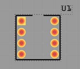
Couldn't have done it simpler.
New Inkscape document:
Canvas dimensions:
- Width: whatever is width of your package in 0.1inch units, plus 0.02in for outline
- Height: number of pads from one side * 0.1inch, plus 0.02in for the outline again
That leaves us with 0.42x0.42in.
By @Radomir Dopieralski's suggestion, let's turn the grid on (View->Page Grid). You can snap to it, which should theoretically decrease the amount of "Transform->Move" we have to do to align everything.
Silkscreen layer:
Draw lines at the contour, for the outline. With the grid, I just drew a path (Straight line tool, draw lines by left click, end drawing by right click). Will see how it works, but it looks great already. Now select the path, group it and ID as "silkscreen". You might also want to color those lines white - while they are selected, point at white in the palette at the bottom and shift-click.
I'd show lines here, but they're white.
Pads:
Pick a color, you'll be drawing pads and this will ensure they're colored as you place them. Just shift-click on any yellow in the palette you'd like to use.
What you'll be drawing is the copper pads exactly the way they'll appear on PCB. I'll just copy the alignment from the sample footprint, shouldn't be
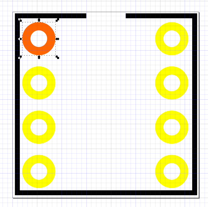
We'll draw first pad in the left bottom corner.
- Set stroke width to 0.02in
- Set width and height to 0.075in
- Set X/Y position to (0.022, 0.022)in
- Make sure it's the right shade of yellow.
Duplicate part and place 3 more pads at X:0.022in, Y:(0.122, 0.222, 0.322)in. Then four parts at X:0322 and same Y coordinates. It's cooler if you overlay a rectangle on top of the first pin's circle to make it a rectangular pad, I won't (I'll make the pad orange and see how it looks in Fritzing).
I also colored the silkscreen lines black for you to see. Looks nice!
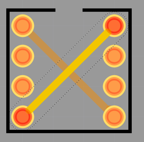
Grouping and IDs
ID the pads as "connectorXpin", where X is from 0 to 7 for us.
Select the pads, group them and ID the group as "copper0". Then select that group. make a group out it and ID it as "copper1". Yes, you should have two nested groups, top group with a single "copper0" group with it. This is a neat trick to distinguish SMD parts from THT parts and show which pad goes where.
If, say, you had an SMD part, you'd only need to use the "copper0" group for your SMD pads. If you had an SMD part soldered to both sides of board (think edge-mounted connectors) and that part had different pad placement on different sides (think of an edge-mounted footprint for a COM port socket), you'd simply put different pads into different groups - top pads into "copper0" group and bottom pads into "copper1" group.
That's it! We've got the main 3 views for a component in 3 short guides. The main thing is - you shouldn't even do all that for the most popular parts, thanks to the parts you can repurpose and edit. On the other side, knowing how to create simple things completely from scratch, you can create a footprint for pretty much any part in Fritzing - such as your custom ESP32 breakout board or another weirdly-shaped module you want to use but don't know how to create a part for.
Discussions
Become a Hackaday.io Member
Create an account to leave a comment. Already have an account? Log In.
You can also change the default paper color in the document properties, so that you can see the white lines!
Are you sure? yes | no