 CYUL
CYULI got the first batch of PCBs back from JLCPCB and found out several mistakes.
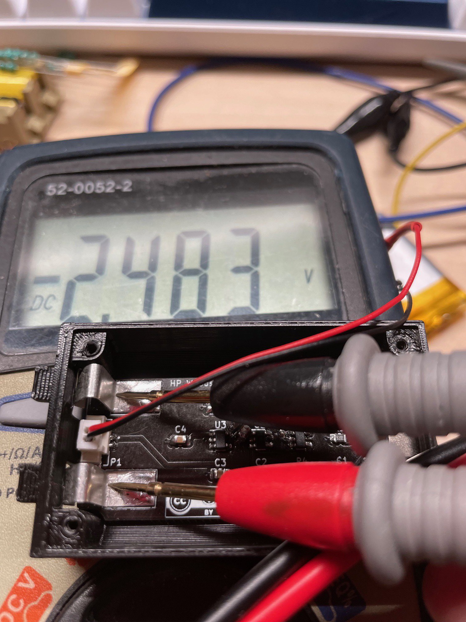
- I had inverted the two 2.5V contacts. Positive is negative and vice versa. I changed my mind in the middle of the initial design and moved the PCB to the bottom of the case instead of right under the top of the enclosure, and this happened... See the minus sign on the multimeter display? Shouldn't be there. Grrrr...
- The spring contacts do not touch the bottom rivet of the contacts inside the calculator. Rather they make contact on the top part of the rivet. It works but barely. I am not sure my HP25 is typical, because that's my only Woodstock, but the contact rivets are very very small. I wonder if it's normal.
- The buck converter stalls when you turn the calculator on (too much current is drawn at once) and only recovers to about 1V vs. its nominal 2.5V
- The 1.25mm connector is way too small. It works with small batteries, the 200 mAh kind that run mini drones, but that won't work for larger batteries, the wire are just too big for those connectors.
So I went back to the drawing board:
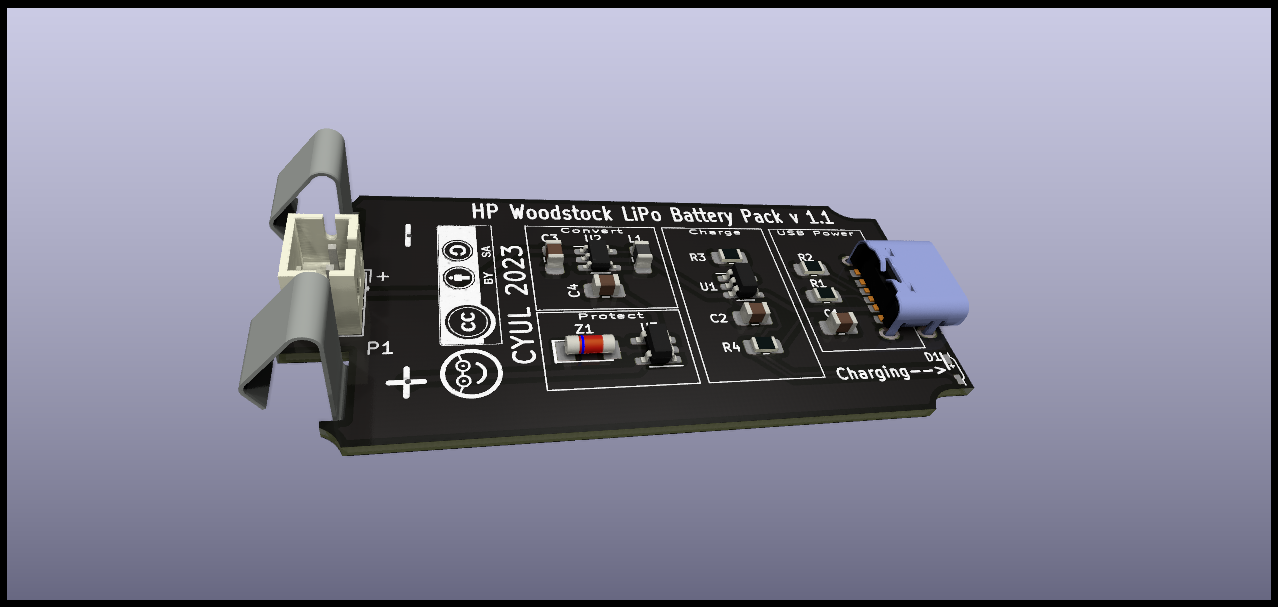
1) and 2) I reworked the PCB to solder the contacts to the bottom of the PCB (and corrected the polarity issue). I changed the outline of the board to hopefully simplify construction. There are notches to guide the contacts when soldering them from the bottom. I wrote + and - in the calculator compartment to remind me.
3) I found someone who had a similar problem with the ADP2108. It turns out, at 3MHz, every millimeter of PCB trace counts. I solved the problem on the prototypes by soldering a 4.7uF capacitor right on the converter pins. Back to the drawing board, again, to change the PCB and shorten the traces. While I was at it, I completely redesigned the layout.
4) I changed the 1.25mm Molex connector for a 2.0mm JST connector. It's going to be tight but it (seems to) fit.
Now there is a new iteration of the enclosure to make space for the battery contact tabs on the bottom (wall thickness has to be at least 1mm, so I just made a hole) and also, since the through hole of the JST connector is smaller than the SMT equivalent, I had to leave space for the two prongs at the bottom of the PCB.
The order for a new PCB is at JLCPCB. Waiting for the first iteration of the enclosure that goes with the 1st PCB. We'll see if that would have worked mechanically.
Discussions
Become a Hackaday.io Member
Create an account to leave a comment. Already have an account? Log In.