 Myk Dormer
L7 is now pretty much fully assembled
Just the EEPROM and the RAM to add, and it's good to go (If it works)
.
No front panel, although a plug on "programmer" board will permit me to modify the EEPROM contents in-circuit
.
.
It's probably sensible to look at the interconnects and assembly
.
I'm using the same high reliability 0.1" pitch sockets and mating square pin headers (as I used on the 162 and the L8) to stack the two main boards, but the programmer board then stacks on top of that I could have used offset mating connectors (as on the 162) but I didn't want to increase the PCB area ...
.
So I've used long pin headers (6mm below the insulator, 7.5mm above) on the upper main board, so a socket can be applied from both above and below
.
(In truth, 7.5mm is too short, as it reduces the inter-pcb gap from the usual 10mm to 8mm. I would use a 9 or 10mm pin by choice, although on the prototype I used what I had in stock)
.
(A keen witted observer will doubtless have sorted out by now that I could have got the best of all worlds by using sockets with long square pins, which then mate into the corresponding socket on the board below, much as the PC104 stacked board systems used. The trouble is that, if I want to keep with the high reliability socket, such variants are very unusual and expensive (Milmetrics might stock one, but I'm not certain) So for now I'm sticking to my current methods
.
.
22/02 First power up. Looks like a +5v rail short circuit
Yes: I am an idiot. The accumulator latch is backwards in its socket, and there is a dry joint on the mask connector. Fix THOSE minor issues and something vaguely hopeful is seen, but with a strangely intermittent power drain (from under 20 to over 40mA, apparently at random, even without the memory chips fitted)
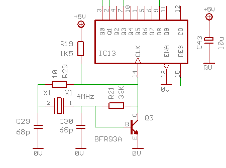
Turns out I have an intermittent (or "sleepy") crystal oscillator. Sometimes it starts up, sometimes it doesn't.
Going back to the circuit I can immediately see the error. The 4MHz clock component values are the ones from the previous design, which used a high speed, low capacitance 32MHz crystal. This design uses a 30pF load 4MHz part. Increase the input and output caps on the oscillator, and increase the loop gain slightly ... success! The clock now runs reliably.
22/02 (later) Load a simple program into the EEPROM (using an external programmer) and I think (only think, mind you) that I am seeing correct execution
24/02 A fair bit of testing and probing, plus some modifications to the pullup and pulldown resistor values in the diode gating, and I THINK we have a workable computer
*** or in other words IT WORKS ! YIPEE!! ***
I have updated the circuit diagram in the main project
25/02 Added a proper block diagram
27/02 With a bit of careful bodging (as the upper board pins are not actually long enough to reliably reach the programmer sockets while the EEPROM is in its socket) I have connected the programmer and I definitely think (from initial tests with a very rudimentary driver on the lab PC) that the in circuit programmer is working
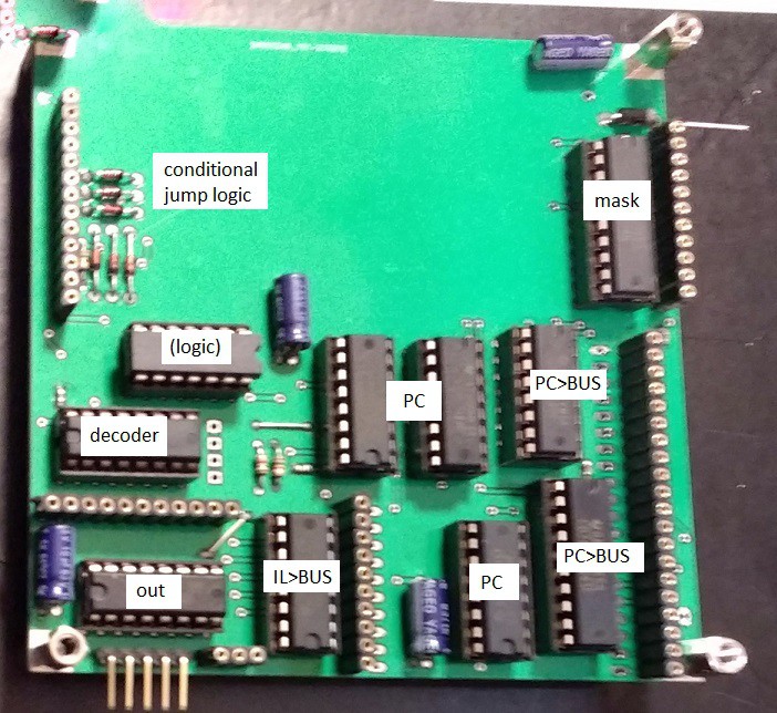
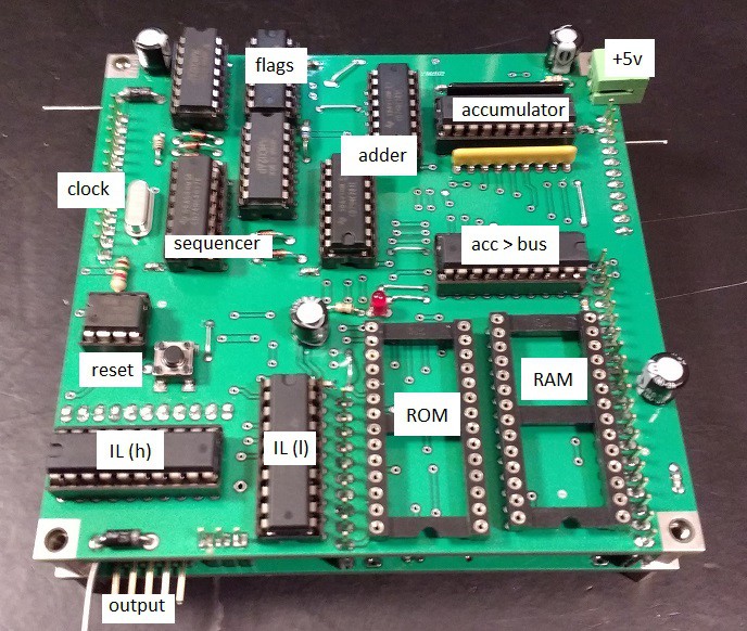
4/03 Annotated images, showing the location of the functional blocks
(the diode gating associated with the ALU is under the accumulator section)
A comment or two
The ROM is a 28C64 (8kx8) part with the highest address bit grounded (a 28C256 could be used)
The RAM is, apparently insanely, a 32kx8 part with all but nine of the address bits grounded ... BECAUSE as of today this is the absolute cheapest way of getting hold of a small RAM.
Everything else is either obsolete, more expensive, or both
 Tobias Rathje
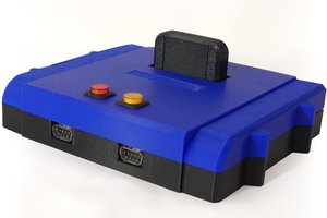
 Clyde Shaffer
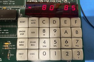
 jimshortz
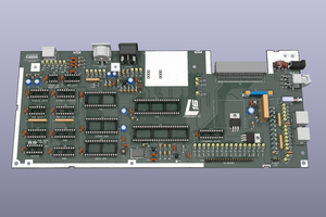
 SukkoPera