 Pierre-Loup M.
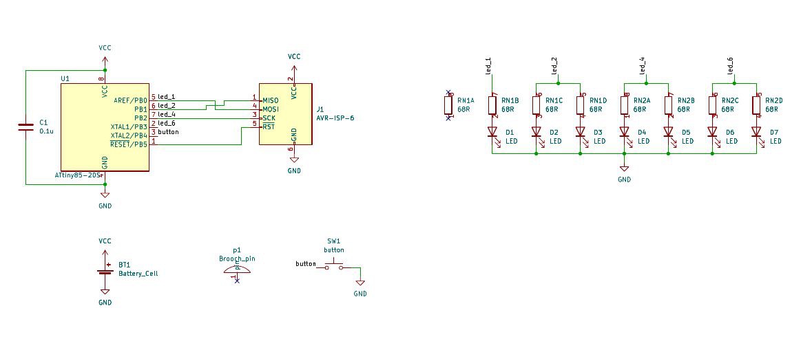
A few details about the hardware. The PCB has been designed with kicad. The circuit is quite simple, the main difficulty is to have everything fit on the small PCB :
- ATTiny 85
- program port (smd pad version)
- 7 leds
- resistances (resistance arrays were used to save surface)
- decoupling capacitor
- a push button
- a cell
- a pin, we want to wear it !
Of course being simple doesn't mean the first one had no problem. In fact it had several issues :
- A track was forgotten, so some enameled wire and hand soldering were used to correct it. Namely, the ground connection of the push button was not linked to the ground of the whole circuit.
- The pin was soldered on a grounded pad, meaning that it could short the cell (and it indeed did !)
- The cell was a CR1015, too small to last long.
- The black color was too sad for the badge.
- Some subtle changes were also made to the outline and the hatch pattern.
The second batch was perfectly fine, with no errors ! :)
Here is the schematics for the badge :
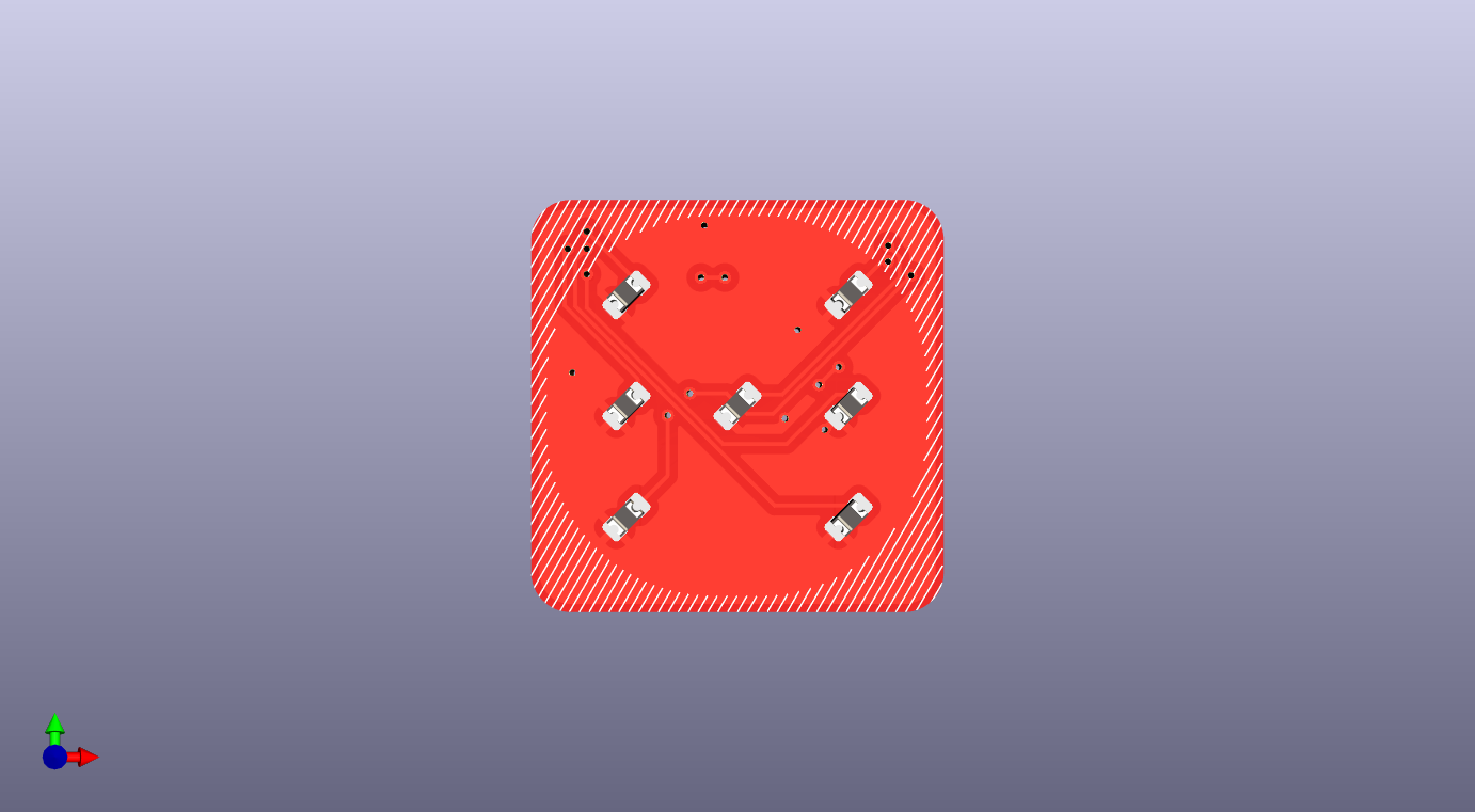
Here is the circuit (viewed from front) :

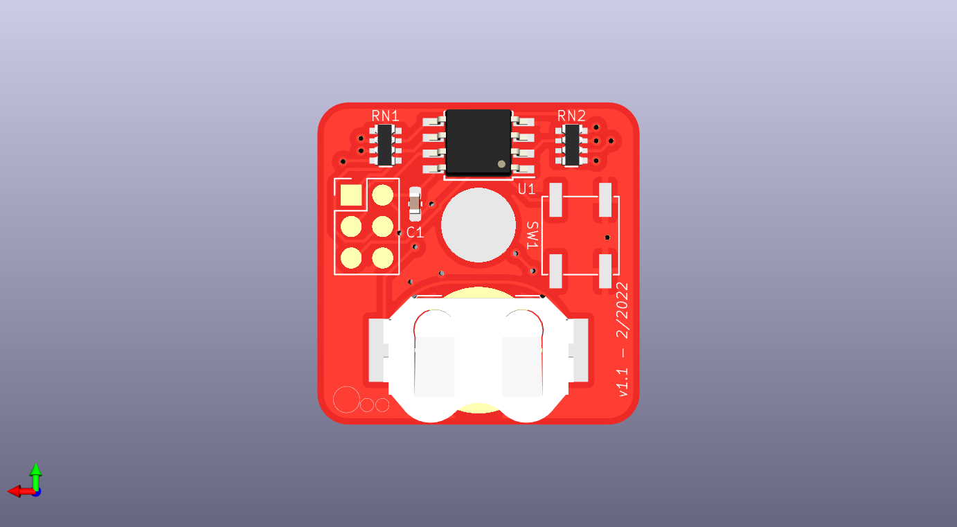
And here are the kicad renderings :
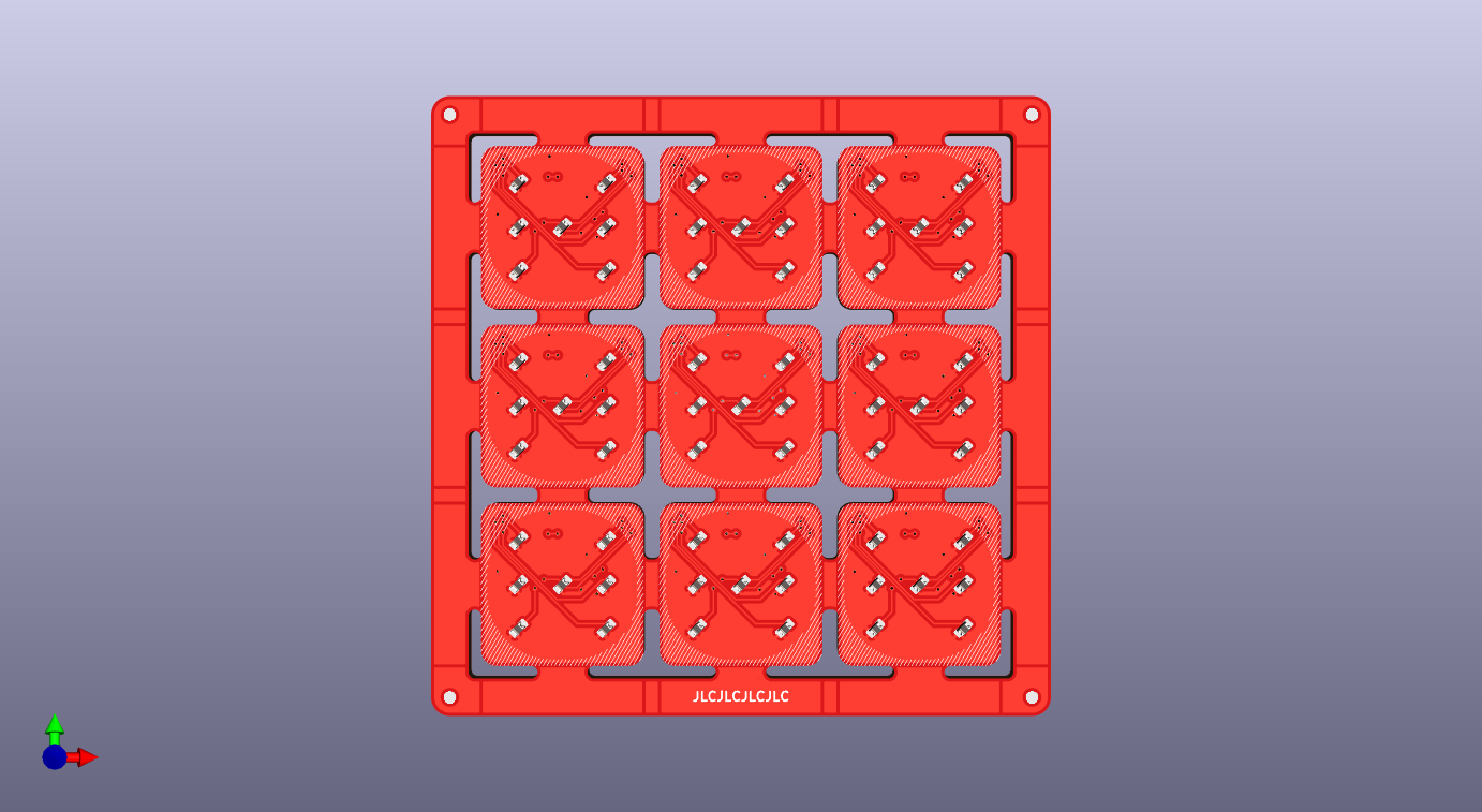
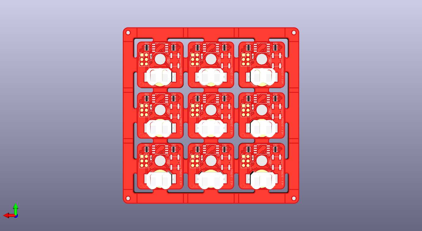
Given the very small size of the PCB, and the fact that most PCB manufacturer bill the same up to 10cm, I've panelized them using Kikit (a tool you might try if you don't know it yet : see it on github).
It's a matter of minutes to have the boards appended to a project, you just run a command again if you have any change to do, it's clean and easy. And it even create the files with the formatting your fabhouse wants. :)
Here is the panelized board, with framing, v-cuts, holes for centering the stencil, and room for JLCPCB to put their internal fab number (you guessed it !) :
Discussions
Become a Hackaday.io Member
Create an account to leave a comment. Already have an account? Log In.