On a couple of solderless breadboards I've build up the CPU and necessary support chips. Then what? Well, we need some memory to test it with but the actual memory layout that I have in mind for the final version is remarkably complex given the 16 banks which can be either EPROM or RAM, the low memory areas which can be either EPROM or RAM and the consideration that the SelfScan interface needs to be able to do what amounts to DMA on the RAM. That's memory number one, and my enthusiasm for debugging that and the CPU itself was, uh, limited.
So let's posit a simple "proof of concept" memory that just has EPROM in the low 8K and RAM in the high 8K. That's memory number two. But for when debugging the CPU what I wanted was something Really Simple. Capital R, capital S.
Therefore we invent "trivial memory". That's just a latch wired up so that whenever the CPU asks to read a byte from memory the latch gates X'C0' onto the bus. X'C0' is a NOP to the 8008. We totally ignore the address bus and we ignore any request to write. With this "memory" in place the CPU simply roars through successive memory locations executing NOPs. That's memory number three. In a sense quite useless but also painfully simple and likely to work, so that's the one I started with.
2023-02-18 Trivial Memory working
Here is a photo of the developments system with the working "trivial memory":
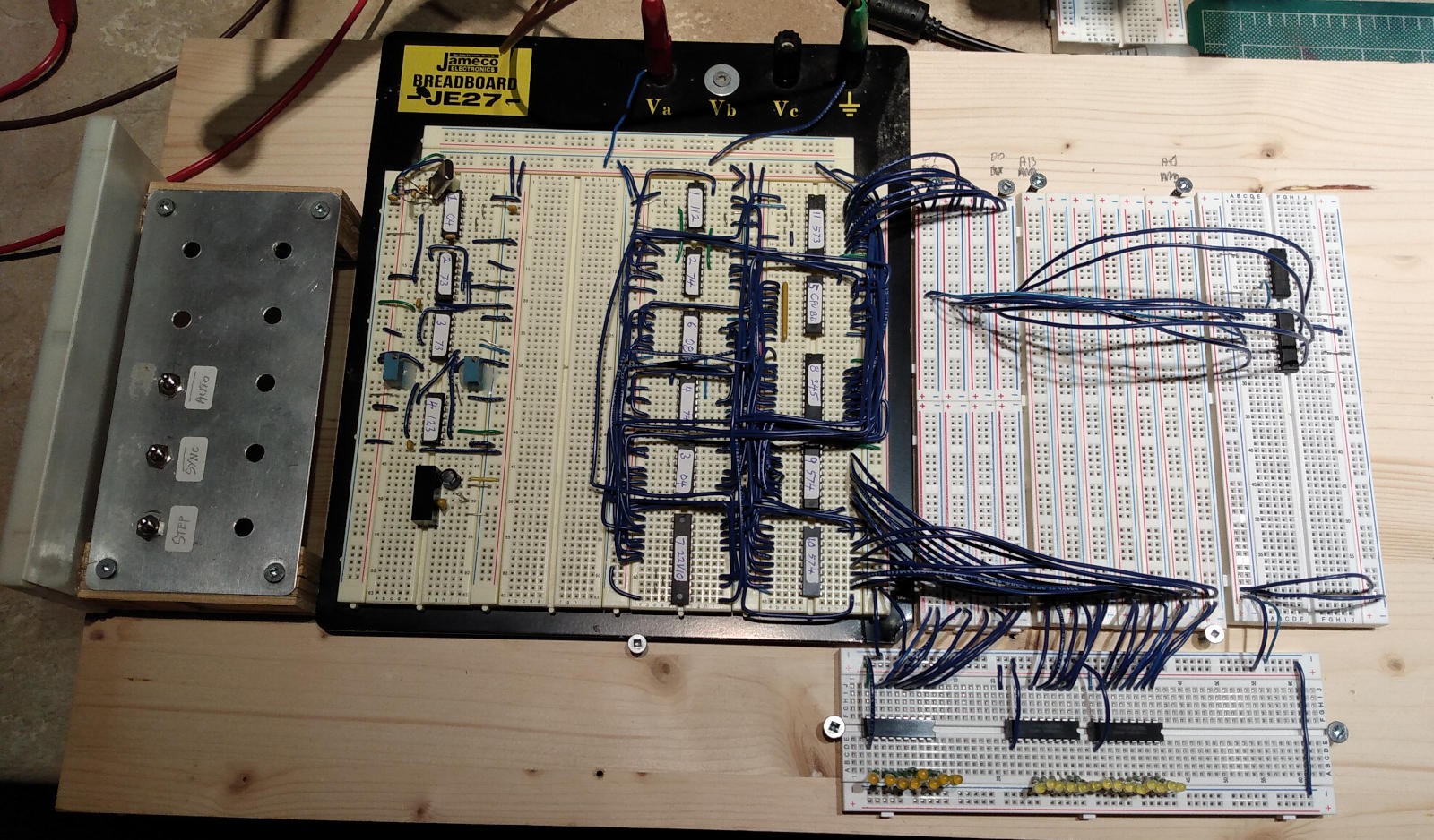
Left to right:
- Three electrically debounced toggle switches.
- First breadboard panel: the 800 kHz 2-phase clock at the top. At the bottom the +5 to -9 converter. Yes, the 8008 requires +5 and -9. But on the bright side, it requires no ground connection. Seriously, there is no ground pin. Apparently it intuits ground based on +5 and -9.
- One blank breadboard.
- Next two breadboards: CPU and support chips. The 8008-1 CPU, very unobtrusive, is in the right hand row, second from the top.
- Four vertical strips which carry the eight data lines.
- Seven vertical strips which carry the 14 address lines.
- Breadboard with the 2-chip "trivial memory"
- At the bottom, a horizontal breadboard with the LEDs that show the address and data lines, and their corresponding drivers.
2023-02-27 - Proof-of-concept Memory working
With Trivial Memory working the next step was Simple Memory. The schematic of the Simple Memory is here (PDF) while the logic for the 16V8 GAL is here. It's about as simple as I could make it while having actual memory. A photo here of the CPU and working trivial memory:
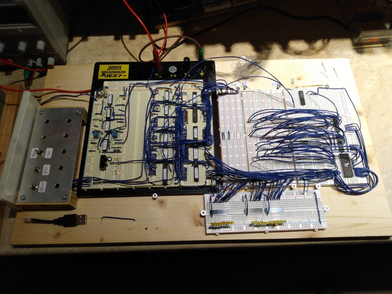
Now over on the right we have a mess of address and data wires. I wasn't too concerned about making these neat and tidy as this memory layout was but a way-station on the way to the real memory. Over on the right is a 64Kx8 EPROM and above that are two 64Kx4 RAM chips. And up above the data+address wires is a 16V8 GAL which supplies the logic glue between the CPU and the memory chips. These memory chips are way more than was is needed for this test, but they are also the chips that I propose to use for the final system, so good to know that they work here.
????-??-?? For-real memory
I've got a preliminary design for the for-real memory, a final design will be forthcoming real-soon-now. But in the meantime I want to get the keyboard looked after - because it will take time to get the PCB produced - and I want to get the SelfScan interface designed because it has to interact with the real memory.
Discussions
Become a Hackaday.io Member
Create an account to leave a comment. Already have an account? Log In.