Close
0%
0%

ISA bus slave NS32016 processor board

By Dave Rand and George Scolaro, 1985.

Similar projects worth following
https://archive.org/details/ns32k-archive is a rich archive of NS32K material.

There is software, and a scanned magazine with articles about building an NS32016 board called the Public Domain 32000. It includes circuit diagrams. It uses 256 kbit DRAM chips, and PAL16L8 chips with logic equations (yay!) but also uses a pair of rare DRAM controller chips (boo!).

I have OCR'd and HTML'd it, and uploaded it for people to download and read. In another language if your browser has translation abilities!

The PD32, was published in Micro Cornucopia number 32, (October/November 1986), page 6.

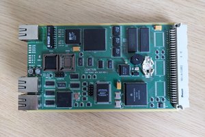
Supports the 32016. Has 512k bytes of DRAM modules.

It is a complete processor board.

It has no bus interface.

It communicates through an 8-bit back-to-back latch. 
This is easy to interface to the ISA bus, or a Z80 bus.
And, I presume, an STEbus or an FTDI USB FIFO module.

It comes with all the PAL equations and software to implement UNIX.

I could not find the DRAM controller chips on eBay, so I presume they are effectively extinct in the wild.
The design could be adapted to use modern SRAM chips. A pair of 512k x 8 bit chips would provide double the original RAM.

The byte-wide communications interface could be adapted to use Jonathon Harston's single-channel Tube API, and thus allow Acorn PANOS to run. But that's a job for people with more time than me.

rom.a32.txt

Boot ROM source code in 32K assembler.

plain - 19.26 kB - 03/11/2023 at 14:40

Download

dram.pal.txt

The logic equations for the PAL that works with the DRAM controller.

plain - 1.53 kB - 03/11/2023 at 13:38

Download

lhu646.pal.txt

This pal generates all the control signals for the 74AS646 data flow latch as well as the CWAIT (for PD32) and IWAIT (for the host) syncronisation signals. The CLK signal is used to clock the data flow flip flop. The GATE signal enables the output of the 74AS646 (the direction comes from a separate ic). The IDO signal is a single status bit that the host can read to determine whether any data is left in the 74AS646 (regardless of direction) or the state of the PD32 service request flip flop.

plain - 2.27 kB - 03/11/2023 at 13:38

Download

646a.pal.txt

This pal generates the control clock signals for the 74LS646 transceivers. Depending on the status of the two flip flops, the pal generates the clock signal for the appropriate 74LS646. The pal also generates CWAIT (for the 32032) if either of the 74LS646's are empty on a read or full on a write.

plain - 2.80 kB - 03/11/2023 at 13:38

Download

dec32.pal.txt

This pal performs the decoding for the 32016 memory space. The signal 'SWAP' is used to select either EPROM or RAM at low memory. At power on or after a reset EPROM is selected at low memory. The EPROM contains the necessary bootstrap software to communicate with the host system (pc). Note: Since the interface is a fairly generic 8 bit parallel port, any system (not just the PC) can become the host for the 32016.

plain - 1.90 kB - 03/11/2023 at 13:38

Download

  • The magazine article

    Keith03/10/2023 at 20:02 0 comments

    Micro Cornucopia number 32, (October/November 1986)

    Public Domain 32000

    By Dave Rand and George Scolaro

    72 Longfellow St. Thousand Oaks CA 91360 (805) 493-1987

    World’s Cheapest Unix System

    Contents

    The Hardware

    This is for all of you who want to put a computer in your clone or CP/M machine. (Sorry, that was a cheap shot.) Actually, this is the cheapest way known to hacker or human to build a truly powerful system (UNIX System V if you wish).

    With hardware floating point that outruns DEC 11-70s, 2 Meg of DRAM, DMA, and a memory management chip, this $400 system is an incredible hardware bargain. See the SOG V article in this issue for information on a public domain operating system for this machine.

    Our primary goal in designing 32000 based system was to come up with a low cost system without compromising performance. One of the unique aspects of the design (which was first presented at SOG V) is that it has been released to the public; schematics, PAL equations, interface software, and the PCB artwork. For this reason, we named our design PD32. (We are, however, restricting commercial copying of the system, see the note at the end.)

    We chose the National Semiconductor 32000 chip set (second-sourced by Texas Instruments) because it’s inexpensive, is a mature product, and was designed to support high level languages. The total cost of both the hardware and UNIX System V, with which the system runs, should be under $1000.

    The version of UNIX available for this board is the full AT&T UNIX System V release 2. The port was performed by ZAIAZ Communications and is AT&T and National Semiconductor approved.

    About The 32000

    The 32000 series includes the timing control unit (TCU), the central processing unit (CPU), the memory management unit (MMU), the floating point unit (FPU), and the interrupt control unit (ICU). Currently four CPUs are available in the 32000 series; they are the 32008, 32016, 32032, and 32332.

    The 32000 series is unique in the microprocessor world in that it is the only family that maintains 100 percent upward and downward software compatibility at the binary level. This compatiblity means the end user doesn’t need to change software when changing CPUs.

    Of the four CPUs, we chose the 32016 for its price and ease of board routing (the board has only two layers). The 32016 still has a full 32-bit internal architecture but has a 16-bit external data path. To reduce pin count both the CPU and MMU multiplex their data and address buses. In other words, data and address information are put on the same set of pins.

    Hardware Design

    Now that we’ve covered some of the background, let’s take a close look at the design. From Figure 1 we can see that the TCU, CPU, MMU, and FPU figuratively bolt together. To understand how the rest of the system interfaces to these four devices, we need to understand the timing of a bus cycle.


    Figure 1. Main Processor Section


    Addressing

    The CPU places the logical address onto the data/address bus during T1 and pulses its address strobe (ADS) pin. If an MMU is in the system (as in this design) ADS from the CPU connects to ADS of the MMU. The MMU then performs any necessary page table lookups and translations, places the physical address onto the data/address bus, and pulses the physical address valid (PAV) pin. This is performed in the TMMU state.

    This pin becomes the system-wide address strobe pin and also connects into the TCU. The TCU, on receiving the ADS signal, generates either a read (RD) or write (WR) signal during T2 and T3. During T2 and T3 the bus becomes a data bus with data either being read or written by the CPU or MMU. The final T4 state is used internally...

    Read more »

View project log

Enjoy this project?

Share

Discussions

Similar Projects

Does this project spark your interest?

Become a member to follow this project and never miss any updates