 Bharbour
This is the local power supply for the project. It will run on anything between about 8VDC and 14VDC in and outputs a regulated 3.3V out. The schematic is labelled as having 5V out, but the output voltage can be changed easily, by changing the value of the feedback divider resistor R1. In this project, R1 is 31.6K, which results in 3.3V out.
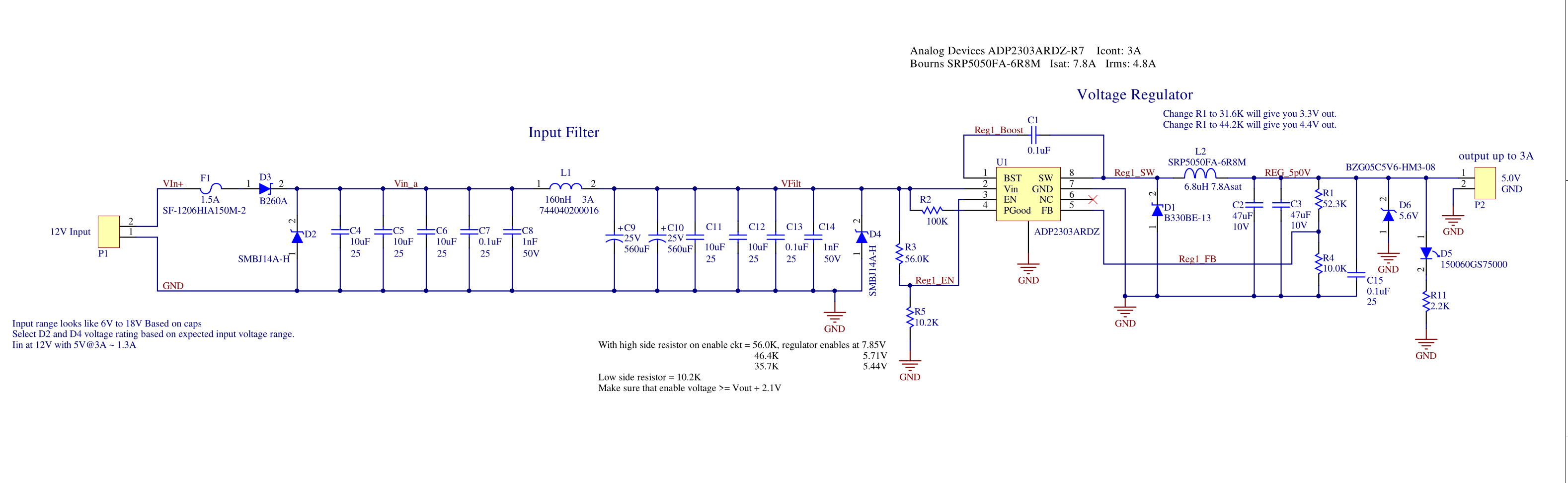
On the left side of the schematic is the input. A fuse protects the input source and to a lesser extent, the rest of the system. The voltage regulator is a buck type switching regulator. Buck regulators have a nasty failure mode where the switching transistor (inside the regulator chip in this design) shorts across. When the switching transistor shorts, it puts the full input voltage on the output of the regulator. Near the right side of the schematic is a zener diode D6 which will start to conduct if the output voltage rises about the specified voltage. If D6 conducts, it will clamp the output voltage to 5.6V, and if the switching transistor has failed, it will blow the input fuse. It is something of a race between the fuse blowing and the diode failing, hopefully the fuse blows first.
Back on the left side of the schematic, there are two diodes next to the fuse, D3 and D2. D3 is a schottky diode to protect the system from a reversed power supply input. D2 is a TVS (Transient Voltage Suppressor) diode which is pretty similar to a zener diode except it is optimized for suppressing fast spikes like ESD events. It will also protect the voltage regulator from over voltage inputs by blowing the input fuse.
After the diodes is a filter. Switching regulators can generate a lot of high frequency energy back into the input side, which in this system is likely to be a long wire to a wall wart power supply. This is called conducted emission. That long wire will radiate that energy, causing problems with any nearby TV or radio equipment. This is becomes radiated emission with the help of the input power cable. The purpose of this filter is to remove as much of that high frequency emission as possible.
In a previous iteration of this board, I had a more complex filter with a lot higher inductance. This made the regulator input look like an inductive load to the wall wart which caused serious startup and stability problems for the wall wart which is another type of switching regulator. The current design does a pretty good job reducing the conducted emissions, and does not irritate the wall wart.
Diode D4 (another TVS diode), after the filter is there to clamp any possible transients created by the inductance in the filter.
Finally, we get to the buck regulator itself. U1 is a variable output buck regulator with the switching transistor in the package. Previous iterations of this board had inductors (L2) that saturated at a current lower than the internal current limiting of the chip. If the inductor saturates, it stops looking like an inductor and destroys the regulator chip and sends the input voltage to the regulator output. The saturation current rating of the inductor used is above the internal current limit and this board design has been operating happily in several systems for a year or more.
Switching regulators are sensitive to the board layout and keeping the regulator chip U1, D1, L2, C2 and C3 very close together is important. The data sheet describes this in detail.
Resistors R1 and R4 make up the feedback voltage divider. The regulated output voltage is divided down to feed back into the error amplifier in the regulator chip.
Diode D6 has already been discussed in the section on the input fuse.
D5 and R11 are just a pilot light to show that there is voltage out of the supply.
The output connector shown has a single + and - output terminal. A later revision of this board has 4 outputs for each. This will simplify the wiring harness construction by avoiding in-line splices on the power distribution.
It is not shown on the schematic here, but the ground (GND) connection goes to the mounting screw pads to connect to the metal chassis ground.
Discussions
Become a Hackaday.io Member
Create an account to leave a comment. Already have an account? Log In.