 Sagar 001
I know the struggle of an electronics student while learning and practicing the digital circuits. In digital circuit we need a lot of external input/ output interface and different clock frequencies. That’s why I designed this digital trainer kit. Which consists of a lot of onboard helping elements. I want to keep it minimal that is why I go with JLCPCB SMT assembly service.
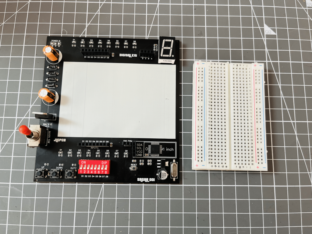
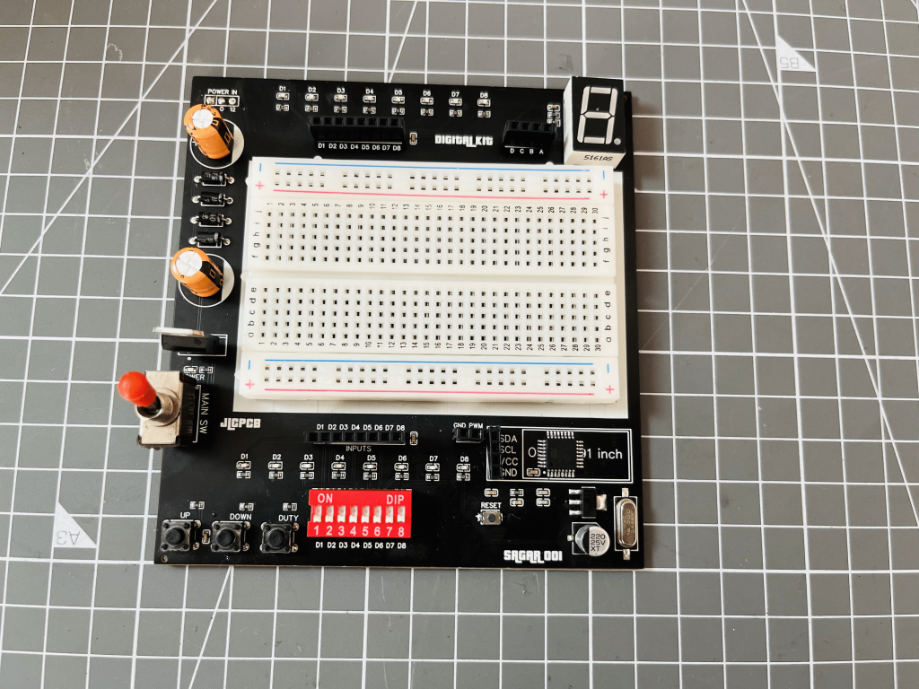
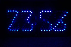
It is the first version of kit which work on a stable logic 5volt. And because of operational amplifier here the kit has dual rail power supply feature. In center 400 pin breadboard space for mounting different ICs. Transformer input, SMD led Input/ output and DIP selection switch for input. Then I added few more features like BCD to 7 segment decoder and CLOCK frequency generator with feedback display.
Here the inputs and outputs LEDs are directly coupled with logic 5 volt but to make it more stable we can add switching transistors to it. And in the PWM/ clock generator a dedicated DDS generator can improve the performance as well as accuracy.
KIT Features:
1) 8-bit input
2) 8-bit output
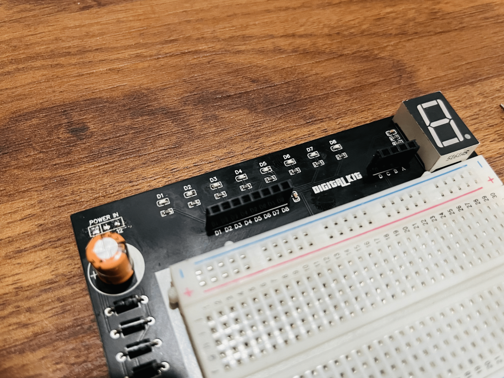
3) BCD to 7 segment decoders
4) Dual rail power supply
5) Headers for power Input/output
6) Clock generator with display
7) 400 pin Breadboard space
8) Minimal size
Circuit Diagram:
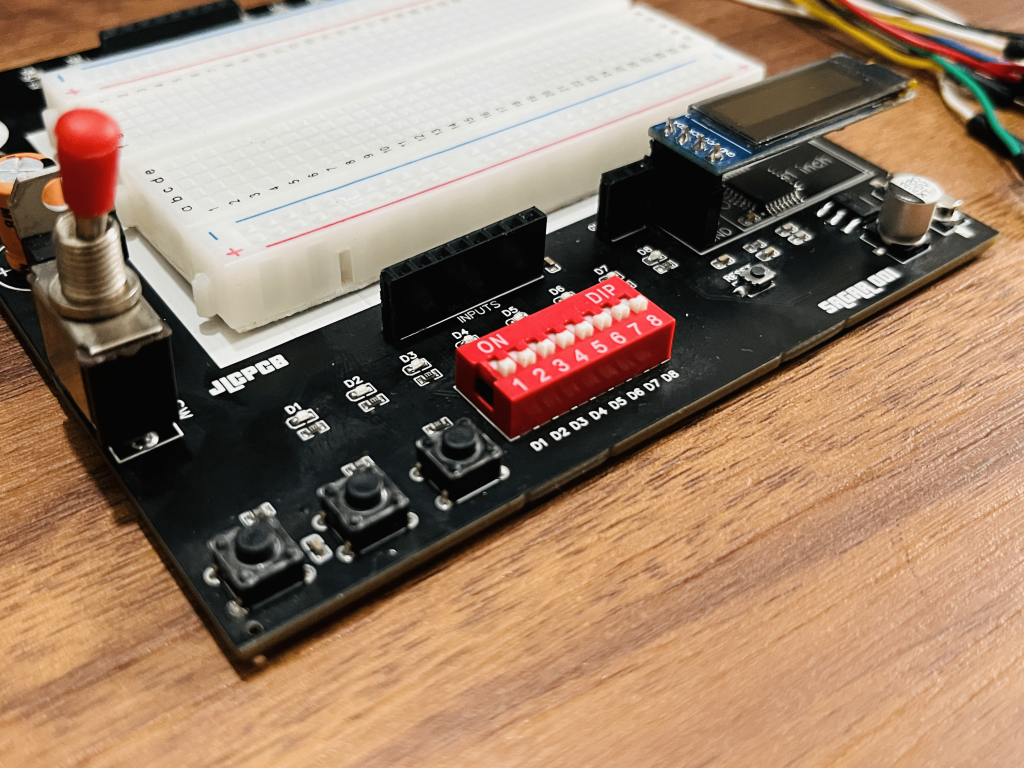
Here you can find the circuit for this kit, I replicate a Arduino Clock generator project in this to make a stable clock for digital circuit testing. This can produce a clock by dividing the Arduino 16Mhz crystal clock in different small units. Duty cycle and frequency of this clock circuit can be selected through 3 tactile switches.
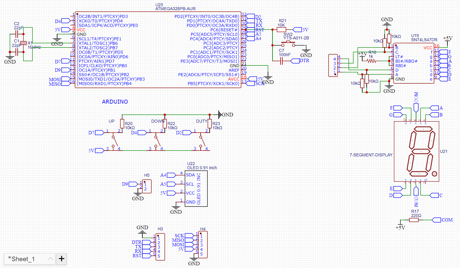
The main reason to get the PCB service from JLCPCB is to minimize the size of board and to get the best quality out of it. The 8 channel inputs and outputs are turned on a logic voltage (not specific one 3.3-7v). Then a BCD to 7 segment convertor (74LS47) is there which is to verify the counter operations. In the power section a 3 wire transformer input pins, full bridge rectifier, dual power supply output and 5volt regulator with on/off slide switch is there. A lot of connections may produce noise which may cause problems in circuit operation and device behaviour which can be reduced by some power line filtering capacitors.
PCB And Gerber Files Design:
The files are designed in EasyEDA and fabricated by JLCPCB SMT assembly, because there are a lot of small components which may increase the soldering and assembling time. JLCPCB SMT assembly simply do a great job the cost of per soldering joint is around $0.004 and PCB assembly services starting from just $8.
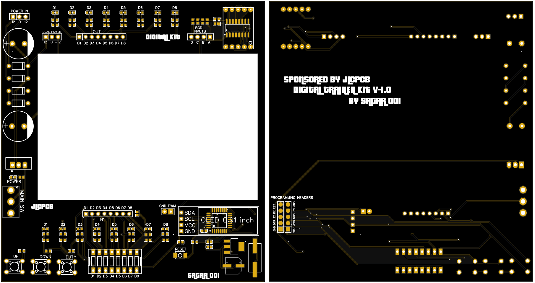
If you want to make this kit here are the Gerber files which can be used to place the order directly. All the info about the code is shared on my GitHub page. Or you can download the PCB files and code from here.
Programming The Clock:
Here Arduino’s atmega328p as a microcontroller is used for the clock interface, and new chip does not have bootloader. First the bootloader is burned through the other microcontroller (Arduino board) and then we flash the code in it. All the programming headers are given in the back side of PCB which can be directly connected to external MCU via headers or jumpers. See from here how to burn bootloader and upload the code.
Arduino Code For Clock:
All the required libraries can be directly downloaded from the manage library section under the tools menu.
#include <TimerOne.h>
#include <Wire.h>
#include <Adafruit_GFX.h>
#include <Adafruit_SSD1306.h>
unsigned long t=1000,f,k=512;// default 1000 μs (1000 Hz), meander, pulse

byte k1,kn,kn1,kn2;
int drive,drive0;
#define SCREEN_WIDTH 128 // OLED display width, in pixels
#define SCREEN_HEIGHT 32 // OLED display height, in pixels

#define OLED_RESET     -1 // Reset pin # (or -1 if sharing Arduino reset pin)
#define SCREEN_ADDRESS 0x3C ///< See datasheet for Address; 0x3D for 128x64, 0x3C for 128x32
Adafruit_SSD1306 display(SCREEN_WIDTH, SCREEN_HEIGHT, &Wire, OLED_RESET);

void...
Read more »

 Ken Yap
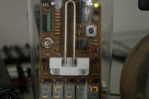
 Kris Slyka
 rawe
rawe
I gonna make a newer version soon, I suggest to order than new one with more interesting features.