Which functions do we need in the ALU and how must that be arranged? Well, we need the usual ones:
Arithmetic:
- ADD (Add two bytes)
- SUB (Subtract one byte from the other)
- INC (Increment: Add 1 to a byte)
- DEC (Decrement: Subtract 1 from a byte)
Logic:
- bitwise AND
- bitwise OR
- bitwise XOR (called EOR for the 6502)
Shifts:
- Shift the bits in the byte one bit to the left (For ROL and ASL on the 6502)
- Shift the bits in the byte one bit to the right (For ROR and LSR on the 6502)
Pass:
- PASS Pass data from databus unmodified.
It must be possible to pass a byte from the databus to the output of the ALU, because otherwise it would not be possible to simply load a value in one of the registers (it is needed for LOAD functions).
The ADDER
The ADD function is easy to realize. There is a chip that can add two 4-bit values, it is called the 74AC283. If we use two of them, we can add two bytes that are present on the A and B input of the adder. The chip has a 'carry' input that can be connected to the Carry flag to provide ADC (Add with carry).
We need a way to connect the A-input of the adder to zero, this causes the B-input (databus) to be added to zero, passing the databus value to the output, providing the PASS function. If we set the carry-input of the adder to logic 1, this function will become INC.
If we connect the A-input of the adder to the value 0xFF (all 8 bits '1'), the adder will add the value 255 to the B-input (databus). But this is a value greater than 8 bits ! The 8th bit will be dropped and the result is that the databus value is decremented, so we now have DEC.
And we need a subtract function, SUB. This can be calculated by bitwise complementing (replacing 0 by 1, and 1 by 0) the B-input, and then ADD (while providing '1' on the carry input). The 'carry' input can be connected to the Carry flag to provide SBC (Subtract with carry).
Left shift can be done by adding a value to itself. The microcode will handle that, so the 6502 or Z80 functions to shift left will work as usual. The right shift needs a dedicated chip.
A simple way to do LOGIC functions
For providing logic functions, the easiest way to do that seems to be to build something like the following circuit:
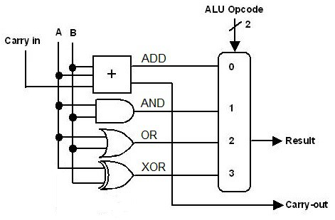
This not only provides the logic functions, but also ADD. It is very easy to understand, the left side of the diagram calculates the ADD, AND, OR and XOR functions, and at the right side the ALU Opcode selects which of the four results will be used (with a 4-input multiplexer). It will work perfectly.
How many parts will be needed ?
Since this is an 8-bit ALU, we need 8 gates of each type. There are 4 gates in a chip, so calculating the three logic functions cost 6 chips. We need eight 1-bit multiplexers, there are two in a chip, so that cost 4 chips, and there are the two adder chips, for a total of 12 for the circuit above.
But there are more chips needed. For subtract, the B input must be complemented, that can be done with two 74HC86 XOR gate chips. And for INC or DEC we must be able to put a value of 0 or 0xFF on the A input. This can be done with two multiplexers 74HC157, that can connect the A-input either to the input bus or to the fixed value 0 or 0xFF. That is 4 chips for these special functions, bringing the total to 16 chips for the ALU.
Calculating Logic functions with less chips
In the previous section we used a multiplexer. It has two inputs X and Y that select one of the inputs A, B, C or D and put the selected signal on its output Q:
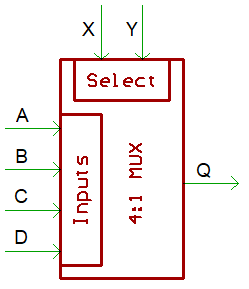
The truth table of this device is:
X   Y   Q
----------
0   0   A
0   1   B
1   0   C
1   1   D
If we now regard X and Y as inputs and A, B, C and D as constants, we actually have a programmable logic gate, where the value on the four ABCD inputs determines which 1-bit function it performs on the values X and Y:
DCBA
0000  Always 0
1000  AND
1110  OR
0110  XOR
1100  pass value X
1010  pass value Y
0011  pass value X complemented
0101  pass value Y complemented
1111  Always 0xFF
This is also explained in this page of Dieter Mueller. So this simple device can do all required logic functions and provides a simple way to select which function it should perform. The same trick was used in the 8086 processor, described in this article by Ken Shirriff about the ALU of the 8086.
There are two of these devices in a 74HC153 or 74AC153 chip. So for 8 bits we need 4 chips ? That would be very nice, but unfortunately, it is not true. Both two internal multiplexers of this chip have the X wires and Y wires connected to each other, as common inputs. So we need 8 of those chips. But what to do with the now unused second device in each chip ? Well, we can build TWO logic units, that share the same inputs X and Y, and that each have their own Q outputs. We then connect both Q outputs to the input of the adder:
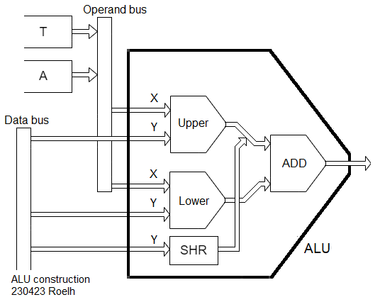
The two logic units are called Upper and Lower. The Upper and Lower logic unit each have their own ABCD control value. Now it is easy to have the extra functions that we need, a complement-circuit for subtraction (in lower logic unit), and a fixed value 0 or 0xFF (in upper logic unit).
The only function that is missing is the shift-right (For ROR and LSR on the 6502), so a SHR circuit that shifts the bits to the right can be used instead of the upper logic unit. For shifting right, the output of the lower logic unit must be zero. [edit 231025 : I later decided that there will not be a SHR unit, to save parts. SHR will be done in microcode, with a table in memory]
The adder will add the results of both logic units. This gives the following functions:
Upper      Lower
Logic      Logic
DCBA       DCBA
--------   --------
1100 (X)   1010 (Y)     ADD Y to X
1100 (X)   0101 (not Y) SUB Y from X (need Cin = 1)

0000 (0)   1010 (Y)     PASS Y (with CY: INC Y)
0000 (0)   0101 (not Y) CPL Y (bitwise complement Y)
1111 (FF)  1010 (Y)     DEC Y

1000       0000         AND
1110       0000         OR
0110       0000         XOR
Note that for all functions, we can swap the ABCD values of both logic units without changing the final result.
The function of the ALU is now controlled by the two 4-bit ABCD values. These two 4-bit values will be provided by the control section of the CPU.
In the control section of the CPU, there will be another multiplexer circuit that uses two control bits to select one of the following four sources for the carry-input of the adder:
- 0
- 1 (Needed for SUB and INC)
- C (Carry flag, needed for ADC and SBC)
- TC (Internal Temporary carry flag, used for address calculations)
This ALU is only 11 TTL chips (10 without the SHR unit), instead of the 16 for the simple design in the previous section.
We are in good company, the same ALU principle is used in the C74 6502 TTL design and in the Gigatron.
Discussions
Become a Hackaday.io Member
Create an account to leave a comment. Already have an account? Log In.
We can reduce the final adder to a simple XOR gate. "Upper" looks about right. But "lower" works better as a Manchester Borrow chain of 5 ohm transmission gates. Arithmetic emerges from a final XOR of "upper" vs previous slice's "lower". Almost per your 230401 drawing, but some connections span between slices.
To ADD, XORvert all Y inputs. But inverted Y also distorts the "Upper" Karnaugh map when we do. The corrected ABCD to use is uniformly NXOR. Map XOR if you prefer inverse Carry or non-inverse Borrow.
CBEQ might represent Carry, Borrow, or EQual. You are familiar with Gigatron's = < > branch control bits, so already know how to setup CBEQo LT GT to compare. Disable all three for logic. From there, let CBEQn+1 = MUX4 ( X, Y, CBEQn, GT, LT, CBEQn ). Repeat.
LT GT modify the behavior of Generate and Annihilate to make X-Y, Y-X, or X+Y. Arithmetic prefixes are decoded inside the MUX, but only observed as switch behavior. Combinatorial MUX like 153 may decode the same internal prefixes, but driven outputs awaiting a valid input can only ripple.
Transmission gate MUX don't have to wait for valid propagation input to begin switching. Consider 74CBT3253 (same pinout as 153) with 74LVC2G86 (dual XOR). Y's initial XOR takes 6nS. All X vs Y decode to switch closures in 6nS parallel time. +250pS per 5 Ohm slice for series current to propagate. Final XOR is 6nS.
Instead of SHR, consider wiring that MUX to reverse 76543210 to 01234567 +250pS (74CBT3257). Leftward propagation without exception simplifies handling of the flag. Next operation may restore orientation or leave reversed.
QBEQo is sometimes a flag, sometimes a control, and often needs override. I would let the raw flagflop choose between a Low Override and High Override using 74LVC1G157. Though this MUX is combinatorial, Initial XOR + Lower won't be ready for 12nS. Plenty of time for CBEQo to enter the chain strongly driven.
-edit- With 230423, you now MUX SHR to "upper". Read my response according to your older 230401 drawing till I get a chance to unscramble what I wrote to match. Would be easier if comments let me embed a drawing rather than try to make sense with only words.
Are you sure? yes | no