The following diagrams will clarify how the information flows in this CPU.
All registers and busses that are shown here are 8 bits wide.
INSTRUCTION FETCH
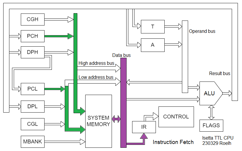
This diagram shows how the opcode of an instruction is fetched from memory. The program counter, consisting of an 8-bit high part (PCH) and an 8-bit low part (PCL), addresses a location in memory where the opcode can be found. This opcode is read from memory and transferred to the instruction register (IR). The instruction register is connected to the control unit, that is responsible for the execution of this instruction. It will do this by executing micro-instructions that are in its own private read-only memory (not shown here). The program counter (PCH/PCL) contains a counter that will increment after the opcode is read.
OPERAND FETCH
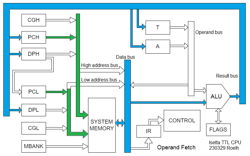
If the instruction has an operand, the operand will be addressed by PCH/PCL. It will be read from that address in memory and will first be transferred to the databus and the ALU. The ALU is in this case configured to ignore the contents of the operand bus, and transfer the contents of the databus to its output without modifying it. The byte then is transferred through the result bus and delivered to one of the indicated registers A, T, DPH, DPL or PCH.
ADD FROM ZERO PAGE TO A
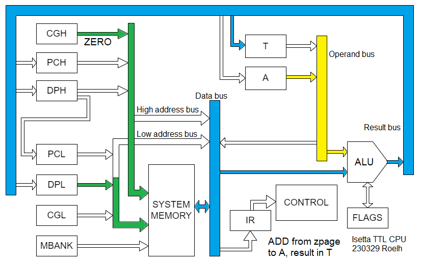
This example shows how an operand in zero page is added to register A, with the result flowing into register T. It supposes that the opcode of the instruction has been read, and that an operand (the zpage address) has been read and has been put into register DPL.
We see here that the lower 8 bits of the address come from DPL while the upper 8 bits are zero. The contents of that memory location is read from memory and transferred to the input of the ALU. The other input of the ALU is equal to the contents of the A register. The ALU will be configured to ADD both inputs, and the result of the ALU is transferred to the T register.
INCREMENT DPL
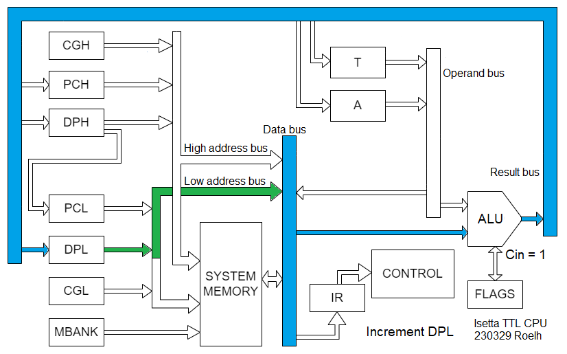
This diagram shows how one of the internal registers (DPL in this case) can be incremented. The ALU is configured to transfer the databus to the result bus (ignoring the operand bus), but the ADDER inside the ALU has its carry-input set to 1, so the ALU will increment the value that is presented on the input.
STORE REGISTER A
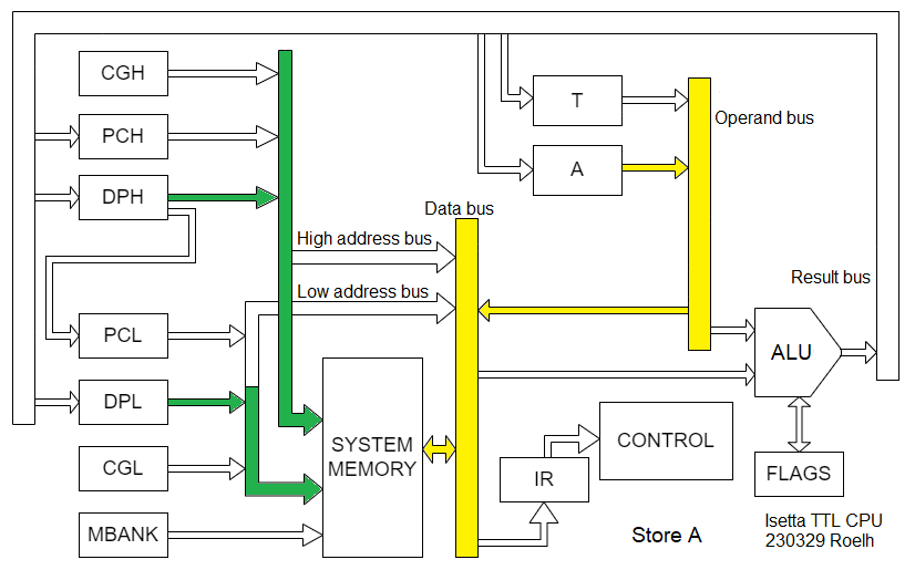
Here is shown how the A register is stored in memory, at a memory location that is addressed by registers DPH and DPL.
Discussions
Become a Hackaday.io Member
Create an account to leave a comment. Already have an account? Log In.