 Frank
Frank
Concept
GM-Study-Max is a FPGA trainer board designed for the Gatemate E1 evaluation board. In 2020, Cologne Chip launched a new FPGA product line, which uses a innovative FPGA blueprint with 8-input LUT trees. For a brand-new FPGA design, it also includes function blocks for JTAG, SerDes, PLLs, dual-port SRAM. Such a market entry is remarkable and deserves to be considered for real-world adoption.
What functions does it have?
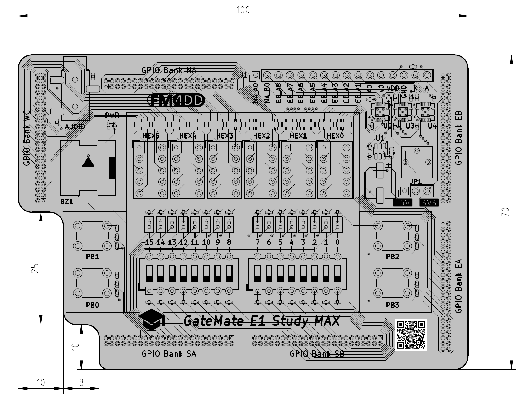
The first design iteration has below set of devices:
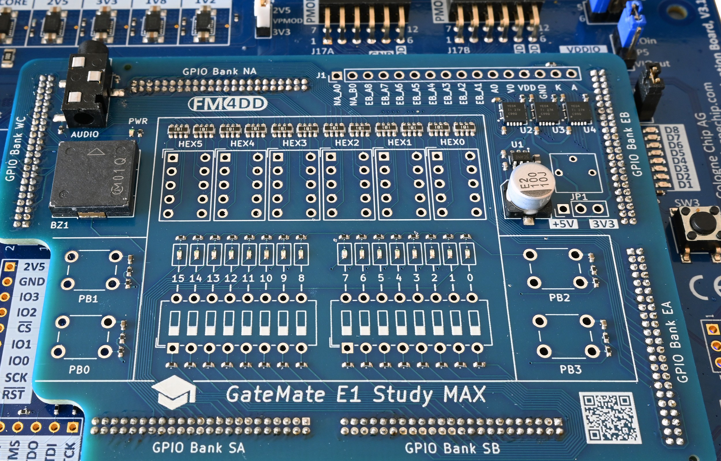
- 4x push buttons
- 16x DIP slide switches
- 16x LED
- 6x 7-Segment display modules (non-multiplexed)
- 1x 4 Khz buzzer
- 1x 3.5mm Stereo Audio jack
- J1 11-pin 2.54mm pitch header with 3.3 or 5V signal translation
Why did I make it?
The E1 evaluation board from Cologne Chip only has a bare minimum of one push-button and 8 LEDs as input/output. This is insufficient to learn a new platform, or to use it in a FPGA training environment.
What makes it special?
Precision Alignment: The application board has to fit exactly into the E1 evaluation board's six expansion headers. This required perfect alignment at hundreds of a millimeter precision to match the 276 pins (6x46pins) at 1.27mm pitch. The Evaluation board's original design envisioned up to six individual expansion boards, which would be too small for any user interface.
Adding to the challenge was a lack of E1 board CAD drawings, which meant that the measurements had to be taken directly from the board itself.
Special care had to be taken to keep space for potentially soldered E1 JTAG and SPI headers, which resulted in the reduced space of the lower-left PCB corner on GM-Study-Max.
The GM-Study-Max daughter board distance from E1 is tight, but additional distance can be achieved by using a different type of 1.27mm pitch headers. Under the typical usage of an FGPA trainer board, the A1 FPGA chip won't get hot, which would otherwise be a problem, with the design preventing the installation of a heatsink.
Signal level translation: Because Gatemate FPGA's operate at maximum 2.5V signal levels, this can be too low for interaction with an Arduino, or for some LCD display types. The onboard power booster translates the signals for the header J1 up to either 3.3V or 5V TTL level. The output signal level can be selected with a jumper (JP1).
Design
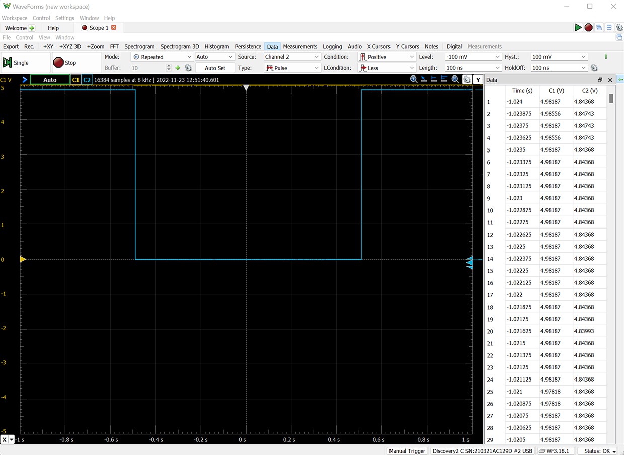
For cost and simplicity, the GM-Study-Max PCB is designed as two-layers only. While this can affect use of high-frequency signals, the trainer board components do not use HF, but run at sufficiently low frequency.
During design prototyping, cost is major concern. It always takes a few iterations to validate the routing, component selection and interaction. For the same cost reasons, I am using a hybrid component assembly, with only SMD components assembled at the PCB Fab.
However, the PCB Fab service is made for high-volume and standard components, which meant I needed to go for a through-hole design on the expansion header connectors. Manually soldering 276 pins at 1.27 mm pitch is taxing my eyesight and needs steady hands.
Production
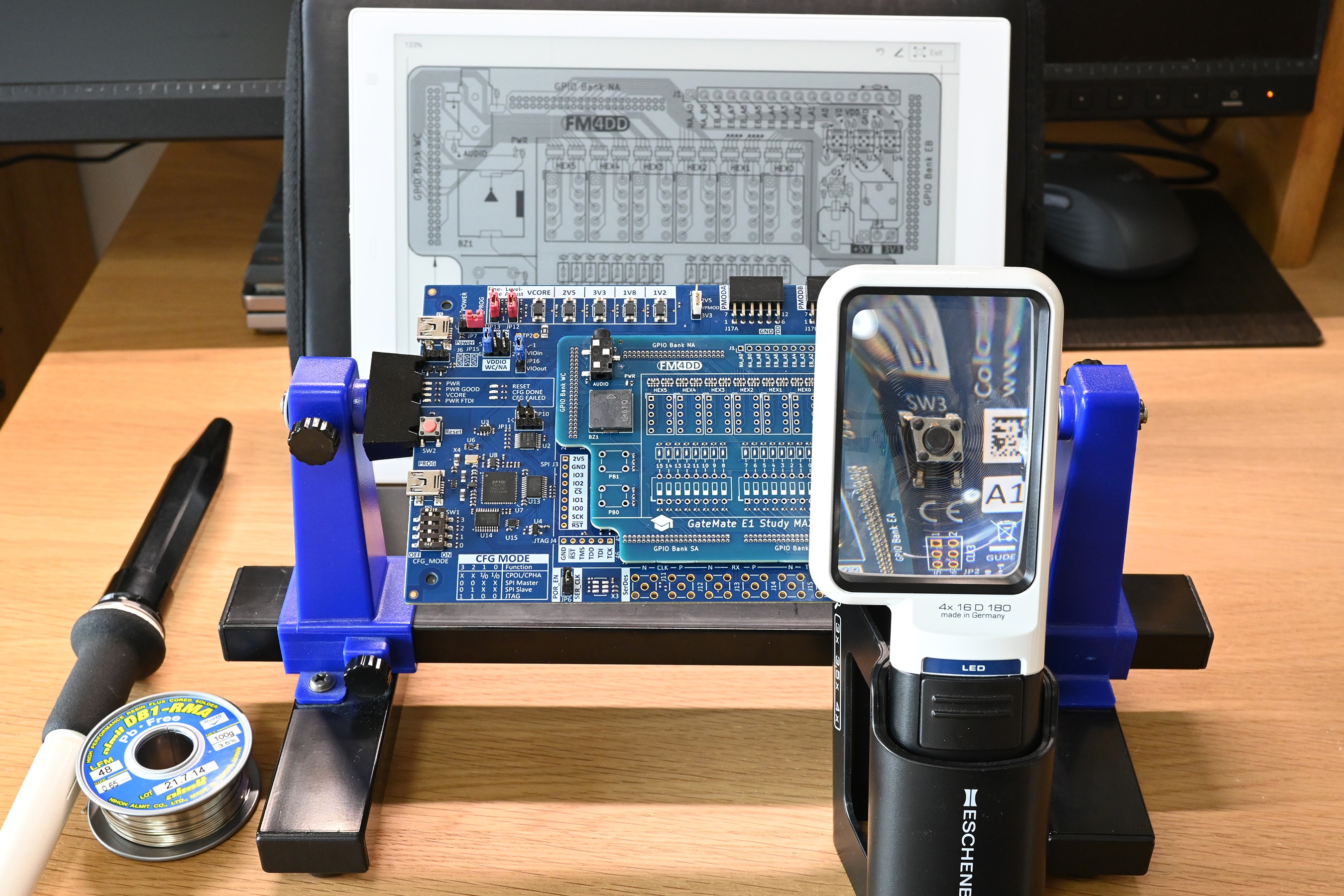
The design documentation is available in the published Github repository. It includes both the fabrication files, and the example code that demonstrate all board components.
License Information
GM-Study-Max is published under Open Source licensing:
- Hardware: CERN Open Hardware License Version 2 - Permissive
- Software: MIT License
- Documentation: License CC BY-SA 4.0
Gatemate FPGA and related products are under commercial copyright by Cologne Chip AG
What is the latest State?
A set of prototype boards have been manufactured, assembled and tested. Photographs and a demo video visualize the board functions. I hope this project shows that Gatemate FPGA's are more than a technology study, and can already be used for real-world applications. The use of an FPGA trainer enables students to become familiar with the advantages of the Gatemate FPGA product line, and its open-source toolchain. This could develop into a viable alternative to market leaders AMD/Xilinx or Intel/Altera, both are restricted to an unwieldy, complex and proprietary toolchain.