 NNNI
NNNIThe multislope ADC's potential 6.5 digit resolution means there are some finer details to the actual implementation.
The first thing is the reference voltage. The go-to choice for high-accuracy bench DMMs is the LTZ1000. Given its price, availability and the large number of expensive supporting components required, it is not the best choice for a DIY approach. The LM399 is a popular part that is used in many 6.5 and 7.5 digit meters. It is more or less a simplified version of the LTZ1000 and costs around 20 Euros in single quantity. It consists of a Zener diode and a heater that maintains the diode at a constant temperature. Applying it is very simple, it only needs a heater supply and a current source to bias the Zener diode. The LM399 has now been superseded by the ADR1399.
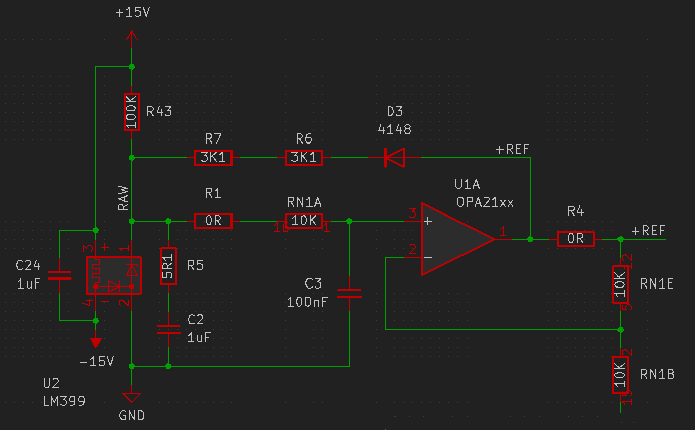
Of course, in real life, the LM399 requires a little care and feeding. The heater pins are connected across the +/-15V supply. While starting up, the heater has a low resistance and can easily draw a few hundred milliamps, which can cause the supply voltages to droop. A constant current source could be added in series to the heater to prevent excessive startup current, but on this board I chose not to add an untested circuit. In normal operation, the heater draws around 20mA. The Zener diode is "bootstrapped" to the reference amplifier output. This ensures a constant voltage across the current setting resistors R6 and R7, leading to a stable Zener current and therefore a stable Zener voltage. D3 and R43 form part of the startup circuit to ensure that the reference does not start up the "wrong way", that is, forward biasing the Zener diode. R43 sets up a small trickle current on startup that correctly biases the Zener diode, after which the op-amp takes over through D3. R5 and C2 can be optionally populated if an ADR1399 is being used, which needs some external compensation to ensure good transient response. R1, RN1A and C3 provide some additional filtering to reduce reference noise.
The multislope requires two equal reference voltages of opposite polarity, which are derived from the reference. Feedback resistors could be selected to provide an exact voltage like 10V, but using a 2:1 divider simplifies the overall circuit and gives the input voltage a little more headroom. There are other ways to implement the bipolar references, like a cascaded non-inverting and inverting amplifier, but I chose the "constant current string" topology.
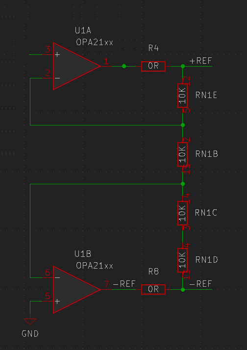
The LM399's Zener voltage is fed into the input of U1A, which tries to maintain the same voltage across RN1B. Since the other end of RN1B is held at ground by U1B, the voltage across it is exactly the reference voltage. Since RN1E, RN1C and RN1D are of the same value, the same voltage is generated across them since the same current flows through them. This means the outputs of each op-amp are at +/- 2x Zener voltage and inherit some of the LM399's stability.
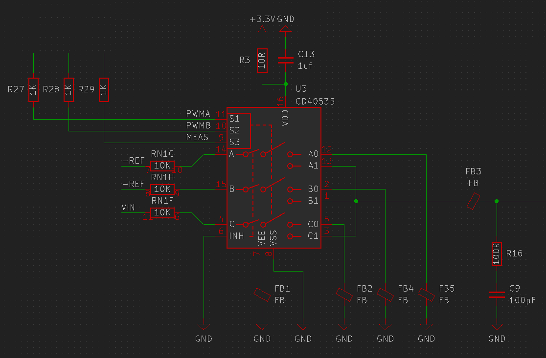
The analog switch is a crucial part of the circuit. My choice was the SN74LV4053 from TI, which is a low voltage variant of the classic CD4053 SPDT analog switch IC. I've tested the LV4053, and it can switch up to several megahertz. Since it can run from a 3.3V supply, talking to it using a Raspberry Pi Pico is easy. The switches in the IC have an on-state resistance of 190 Ohms with a 3V supply and 30 Ohm matching between channels. Temperature coefficient is not specified. It is important that the analog switches have an on resistance that is much smaller than the V-to-I resistors. In this case, the latter are 10 kiloohms, so a 190 Ohm on resistance represents 2% of their resistance. Supposing the switches have a 5%/K temperature coefficient, the overall variation with temperature is just 0.0005%/K (5ppm/K), not including the temperature coefficient of the V-to-I resistors themselves. The ferrite beads prevent switching artefacts from making their way into ground or the summing junction, and the 100R/100pF filter serves to filter charge injection spikes. R27, R28 and R29 prevent the fast rising and falling edges of the control signal from affecting the analog portions of the circuit. Another point to note is that since the reference voltages are approximately +/-14V, an input voltage range of +/-10V or +/-12V is reasonable, and the same resistor value can be used for the reference and input V-to-I conversion.
There is one secret ingredient that helps enhance stability in both the reference amplification and V-to-I conversion sections: the resistors. The reference designator "RN" is already a dead giveaway - the reference amp feedback and the V-to-I conversion resistors are part of the same network. The resistor networks used in most DMMs are custom, but good integrated resistor networks like the LT5400 and NOMCT1603 can be bought for a few Euros each.
| Parameter | LT5400 (A-Grade, 0C to 70C) | NOMC |
| Absolute accuracy | +/-7.5% | +/-0.1% to +/-1% |
| Ratio accuracy | +/-0.01% | +/-0.025% to +/-0.1% |
| Absolute temperature coefficient | -10 to 25ppm/C | +/-25ppm/C |
| Tracking temperature coefficient | +/-1ppm/C | +/-5ppm/C |
| Excess current noise | < -55dB | < -30dB |
The LT5400 clearly wins in terms of ratio accuracy, temperature coefficient and excess noise, but is available only in networks of four, while a single NOMC has 8 resistors, which fits well with the 7 minimum resistors needed to implement a simple multislope. Resistors from the NOMC family also find use in the Keithley 2002 ADC. Nikolai Beev from CERN wrote a comprehensive paper comparing the excess noise performance of various resistor network families. Both the NOMC and the LT5400 have a noise index of less than -60dB.
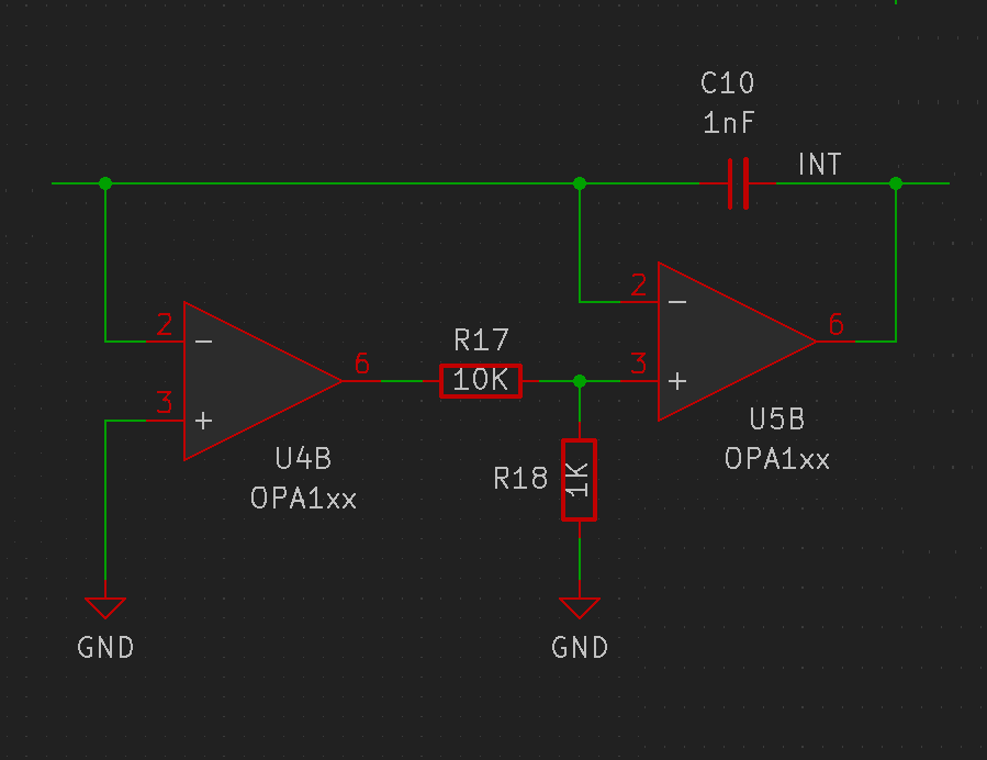
Fast slopes require op-amps with a large bandwidth. Fast op-amps are usually not DC accurate, with offset voltages in the millivolt range. An offset voltage on the integrator shows up as a reference mismatch and can affect readings. Precision op-amps usually have poor high-frequency performance. The composite integrator configuration combines both DC accuracy and high speed. The input stage op-amp is of the precision variety, exhibiting low offset voltage. It closes a feedback loop around the fast output stage op-amp to ensure DC precision. The voltage divider acts to reduce the bandwidth of the precision op-amp by requiring a higher swing on its output to drive the non-inverting input of the output stage op-amp. This somehow also has a positive effect on loop stability, which I don't fully understand - more research and testing is needed in this area.
As for the choice of parts, both the op-amps are the OPA140, which is the current voltnuts' choice thanks to low input bias, low input noise voltage, high offset stability, and very good CMRR. They also have a reasonable 11MHz gain-bandwidth product and a 20V/μs slew rate.
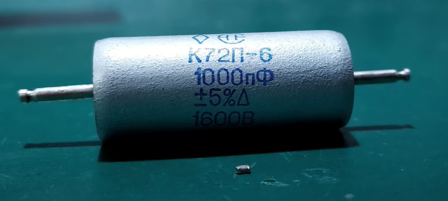
At the center of the whole show is the integrating capacitor. As previously established, reading accuracy depends on the capacitor having low temperature coefficient and low dielectric absorption. This naturally rules out electrolytic capacitors. High-K ceramic capacitors have unacceptably large temperature and voltage coefficients. Film capacitors, particularly polypropylene and polystyrene, are probably the best choice. There is one other rare type of film capacitor that uses a Teflon dielectric, which have the smallest measured dielectric absorption. However, they have very poor volumetric density and are hard to find and therefore very expensive. Low-K ceramic capacitors show marked improvements over their high-K counterparts, and one type, designated C0G, is the best among them. C0G has a 0ppm (+/-30ppm) temperature coefficient, and dielectric absorption almost as low as Teflon capacitors. Most importantly, they are cheap, easily available and small. Here's an 0603 1nF C0G capacitor compared to a 1nF Soviet-era Teflon film capacitor:
Most multislope ADCs also feature slope amplifiers. As their name suggests, they amplify the integrator waveform, which speeds up the zero crossings. Since the integrator swings between a large range, slope amplifiers are usually diode-clamped. Two variants exist, a non-inverting one with a unity large signal gain, and an inverting one that clamps to +/- one diode drop. The non-inverting type is more common, since it preserves the integrator waveform while speeding up zero-crossings.
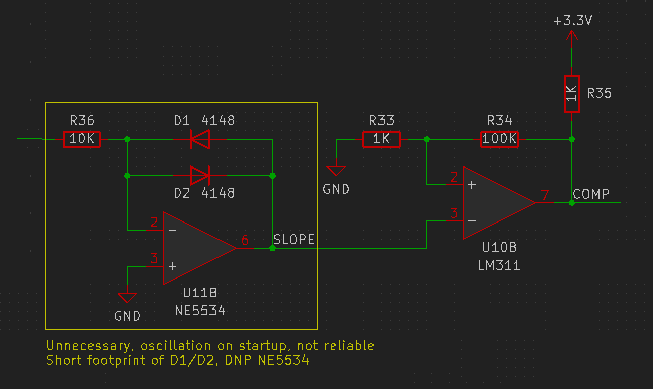
I chose to use the inverting clamping configuration, since I discovered that the LM311 comparator has increased propagation delay when one input is allowed to slew well beyond the reference input. In practice, the circuit I implemented tended to latch up or oscillate, so I ended up bypassing it. The comparator itself, the LM311, is the fastest of the jellybeans, with a 160ns propagation delay. It can also be powered from +/-15V and has a large input common mode range, which simplifies sensing, since no level shifting is needed. A few tens of millivolts of hysteresis also ensures consistent comparison.
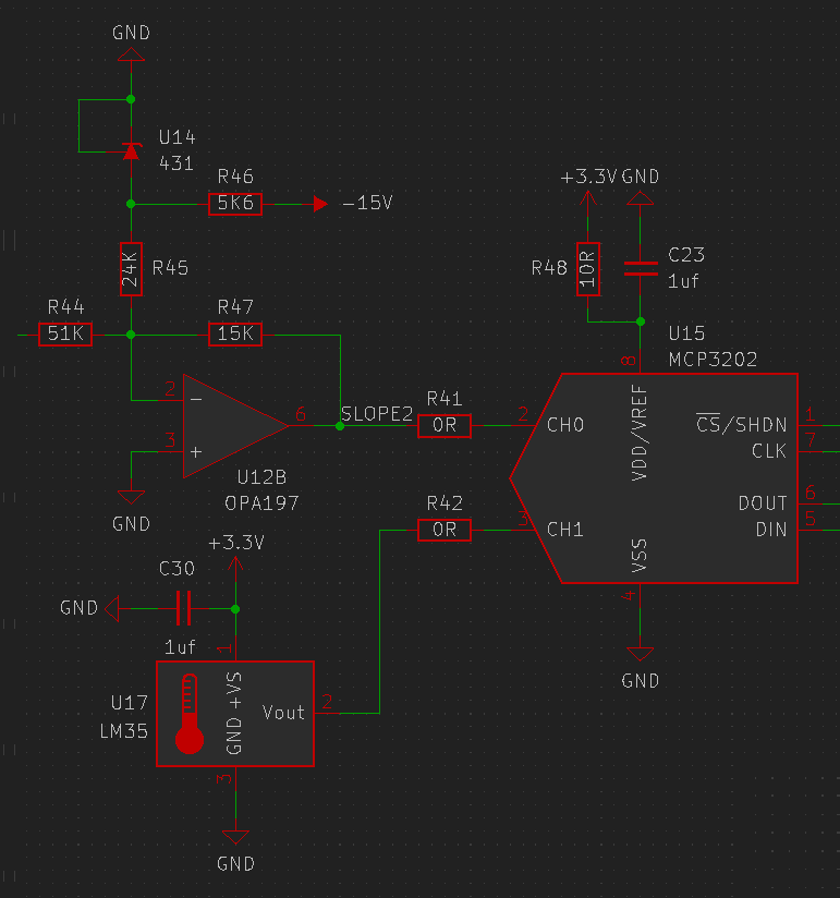
Another powerful technique is being able to measure the actual voltage on the integrator. Even if the input voltage is integrated for one clock cycle, the difference in integrator start and end voltages should still give the correct value for the input voltage. If the integrator voltage is measured before and after a conversion, the difference provides extra resolution to the readings, much like the Vernier scale on a set of Vernier calipers. For this purpose, an MCP3202 ADC is connected to the output of the integrator through a precision scaler that scales the +/-10V integrator swing to 0V - 3.3V that the ADC can digitize. An LM35 temperature sensor (which was designed by the LTZ1000's designer and was his favourite chip) was also added to the second channel of ADC for local temperature measurement.
Now that the references, amplifiers, integrator and comparator have been provided, a programmable digital device is needed to close the loop and keep track of the integrator charge. An FPGA or CPLD has traditionally been used to carry out this task. They are also completely alien to me, expensive, and have extensive toolchains. The initial approach Dmytro came up with was to use the SPI hardware on the Arduino Nano, which was strangely suitable in that it generated clock pulses for and read the state of the flip-flop being used to drive the integrator. The only catch was that the SPI transfers could only be one byte long, so every eight clock cycles there was a gap where the integrator charge was not counted.
The then newly released Raspberry Pi Pico was touted as a solution. It soon became clear that the PIO peripheral was perfectly suited to the task. The D flip-flop could be done away with and the PIO could be used to directly drive the analog switches and also read the comparator output.
One last problem left to solve is that of charge injection. Analog switches are universally based on CMOS processes. The switches are constructed using a complimentary NFET/PFET pair that facilitate bidirectional current flow. Since FET gates are capacitive, the rising edge of the control signal causes a short current spike that makes it to the drain and source terminals, one of which the integrator summing junction is connected to. Every time currents are switched in and out of the integrator, a small unknown charge is added to or subtracted from the integrator. Over many clock cycles, this unknown charge accumulates and causes errors. The non-deterministic nature of the switching and the dependence of charge injection on supply voltage and other conditions makes this error hard to account for.
There is a clever solution to this problem that dates back to the LD120/121 ADC IC set, whose datasheet also provides insight into multislope operation. This involves using complementary PWM signals to drive the reference switches, with two fixed duty cycle values, for example, 20% and 80%. Regardless of input voltage and integrator levels, PWM provides a constant number of switch transitions. This makes calibrating charge injection errors out a relatively simple process.
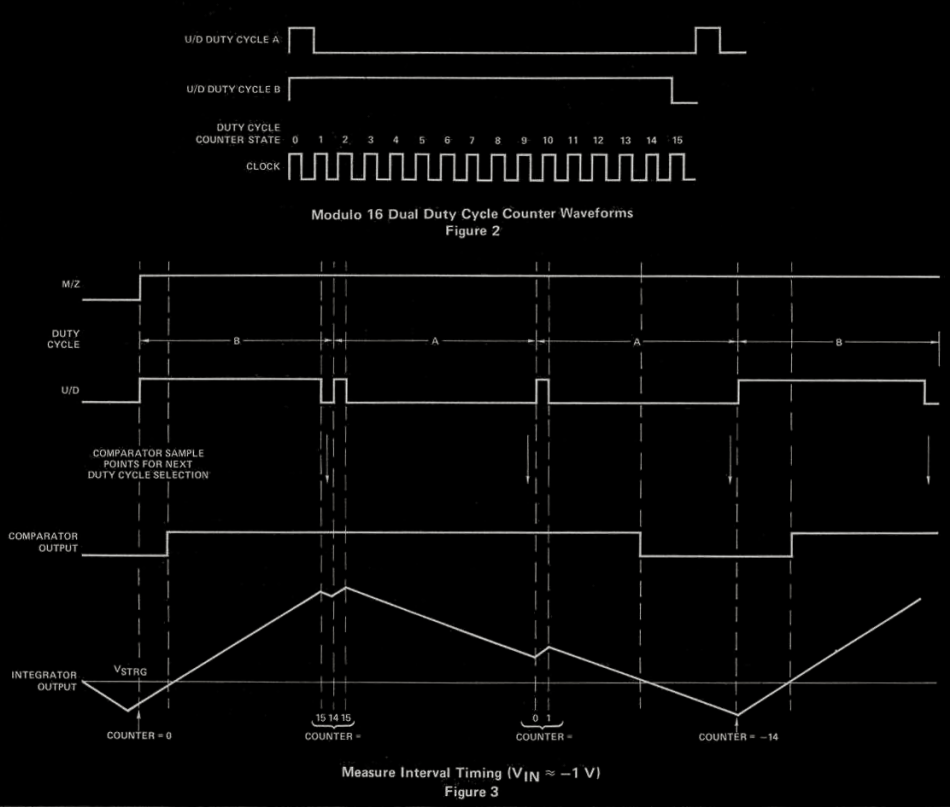
(LD120/121 datasheet, page 3-17, figure 2, 3)
What happens between integration cycles also matters. If the integrator is allowed to drift because of switch leakage, op-amp bias currents or other environmental factors, the output saturates. When the next conversion cycle starts, the integrator takes time to come out of saturation, which affects results. The integrating capacitor's dielectric also soaks up a lot of charge, further affecting readings. Ideally, the capacitor is shorted between conversions, but implementing a shorting circuit is difficult. The HP/Agilent/Keysight 34401A solves this problem by running the integrator constantly, and only counting when a reading is needed. This would be somewhat difficult to implement in PIO, so a different strategy called dithering (described in this paper along with an interesting rundown method) is implemented, which switches the reference currents quickly to maintain the integrator output around zero.
The end result of painstaking testing and debugging was the third iteration of the multislope ADC, called Multislope 3I.
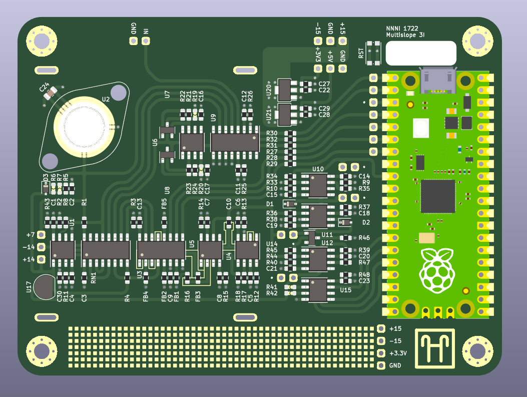
The PCB layout style was the result of working with Mark on a precision DAC project. I have taken to the neat rows of ICs and passives. Curved traces are electrically unnecessary but result in a product worth looking at. There were surprisingly few teething issues since this was the third PCB I'd made for this project and most of the basic bugs had been ironed out, although a few turned up during testing.
The biggest one came from the MCP3202 residue ADC. The raw output readings were noisy and had significant banding. The reason remains unknown, but PCB layout or a software bug is suspected. This led to the RP2040's built in ADC being used, which reduced noise to a large extent.
The second one involved calibration of conversion constants. If the constants are not chosen correctly, the readings have significant banding. Some fine-tuning using MS Excel fixed the problems.
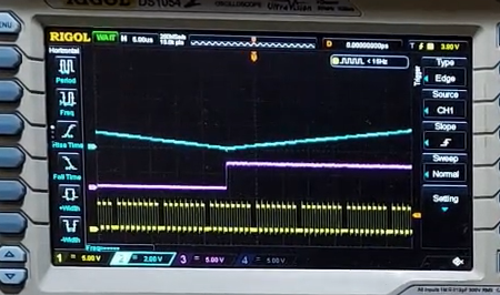
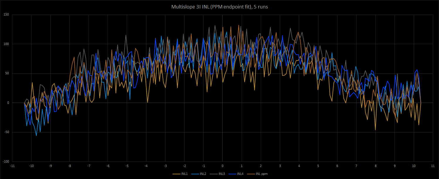
In the time I had to characterize the ADC, I was able to determine that 6.5 digit resolution had probably been achieved, but the readings were quite noisy, and the linearity had an inverted parabolic shape to it. This is a good sign, since the errors is not random and a cause can probably be determined. The spikiness of the data, however, is a bad sign, since it means the readings are quite noisy.
Discussions
Become a Hackaday.io Member
Create an account to leave a comment. Already have an account? Log In.