Klaus Dormann
Hardware
The logic probe is intended to be built on a perfboard, so there is no board layout.
I chose an ATTINY26 for this project simply because I had one. However, it should be possible to port the project to smaller or newer ATTINYs if needed. The AVR must have
- an analog to digital converter
- an external interrupt pin configurable to detect both edges
- a timer with output compare match toggling an output pin
- a second more simplistic timer to generate a timer tick
- 5 additional I/O pins for 3 LEDs, 1 switch and 1 output to precharge the probe
The fuses of the microcontroller should be set to run on the 8 MHz internal oscillator.

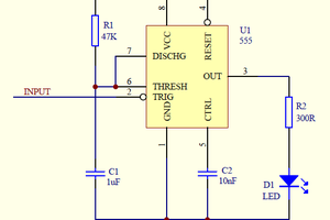
The resistor network R8, R9 & R10 precharge the probe through R1 with a voltage suitable to detect an open circuit. The voltage to signal an undefined logic level is 1.4V for TTL and 2.5V for CMOS. Port A Pin 6 drives R9 high in CMOS-mode, hi-Z in TTL-mode.
The LEDs should be low current types as their resistors allow 5mA at 5V per LED. It is up to you to choose the colors you want to signal high, low or pulse. The sound output device is a magnetic transducer with 40 Ohms impedance. If you have to replace the BJM 05 with a different type, it should not have a lower impedance. Otherwise you might need to add an amplifier.
The switch S1.1 disconnects the speaker if the sound annoys you or your co-workers. The switch S1.2 selects TTL-mode if on, CMOS-mode if off. If you do not want TTL-mode just leave port A pin 7 disconnected. At the same time you can leave pin 6 on the same port also disconnected and bridge R10 (connect R9 directly to Vcc).
The Logic Probe takes its power from the circuit under test. Be careful not to operate the microcontroller outside of its specified operating voltage. Do not reverse Vcc and Ground leads!
Software
For all my AVR assembler projects I use an include with macros to allow me to better structure programs with IF-ELSE-END and DO-EXIT-LOOP blocks. I have written the macros in 2010, they are called "Structured Assembly Macros" and live in "sam.inc".
The program is very simple as it does not use any interrupts or subroutine calls. I still load the stack pointer though, because it is good practice to do so. The reset code then goes on to initialize
- the oscillator calibration register
- timer 0 as an 8ms tick timer
- timer 1 as the frequency generator for the sound
- LED pins, perform a 1 second all on to verify LEDs are O.K.
- the ADC to take its reference voltage from Vcc, output 8 bits to the ADC high register, use ADC9 (port B pin 6) as input, use 125kHz as ADC clock and start free run mode
- to set the INTF0 flag on both edges detected on INT0 (port B pin 6)
- registers for sample counts, edge timer, current logic state frequency
The main program loop consists of 3 major blocks, AD conversion complete, 8ms timer tick and signal edge detected.
The ADC block first decides which levels apply by checking the CMOS/TTL switch. The ADC result sets the high or low LED and counts the samples from last 8 ms timer tick. Finally the probe precharge voltage level is set.
The 8 ms timer tick block first checks whether the 100 ms pulse LED on timer is expired. Then the sample counts and pulse timer determine if the sound should be enabled and which frequency should be used. The last frequency is verified with the current selection and if it is the same the pulse timer gets priority. This causes the sound to warble when a pulse is detected with at least one valid logic level.
In the last block the external interrupt flag is checked and if set turns on the pulse LED and loads or reloads the pulse LED on timer with ~ 100 ms.
Limits
The ADC takes almost 10.000 samples per second when running at 125kHz in free running mode. In the first of the 13 cycles of an AD conversion the sample and hold capacitor is charged from the ADC input pin. Whatever mix of levels is present during that cycle is averaged and then converted. A cycle is 8 µs at 125 kHz. However, only the last 5 µs of the sample cycle are relevant...
Read more »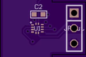
 Electroniclovers123
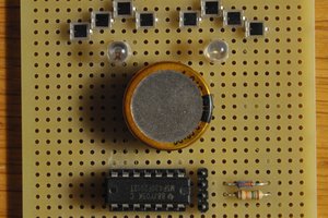
 Matthias Koch