 Mitsuru Yamada
1-1. Configuration of the CMOS simple discrete operational amplifier
In a previous my project, an experimental op-amp module with five bipolar transistors was introduced, and a similar configuration structure with five MOSFETs is used for this CMOS operational amplifier OPM-03. Because of the limited variety of single MOSFETs available and the fairly large variation in Vth, I thought it would be difficult to bring each internal part to an operating point that would allow overall operation, even if more FETs were used to improve the characteristics. Therefore, in this homemade project, it was decided that even if the characteristics were inferior to those of commercially available monolithic ICs, it would be sufficient if I could manage to achieve operation as a CMOS operational amplifier and experience its features.
Figure 1 shows the circuit of OPM-03. The internal circuit consists of three stages: the first stage is a differential pair, the second stage is a gain stage, and the third stage is a source follower. The MOSFETs used are 2N7000 for the N-channel type and BS250P for the P-channel type, both of which are for low-power switching. The datasheet states that the Vth value varies from 0.8 V to 3 V.
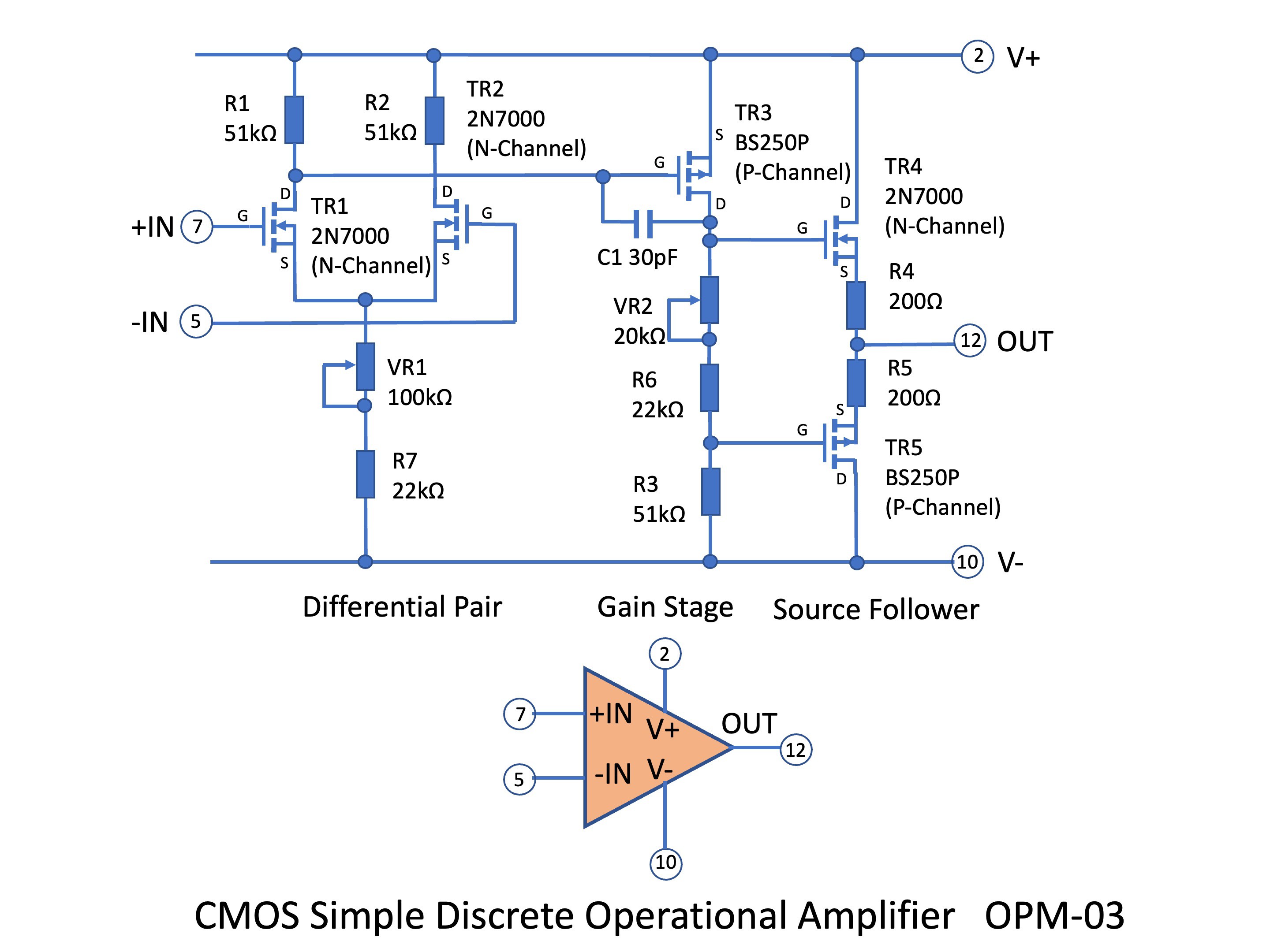
Fig.1 Circuit of the CMOS simple discrete operational amplifier
Figures 2 and 3 show the appearance of the homemade CMOS discrete operational amplifier. The external dimensions are the same as the op-amp module of the previous project, 30 mm x 30 mm, and the pin layout is the same.
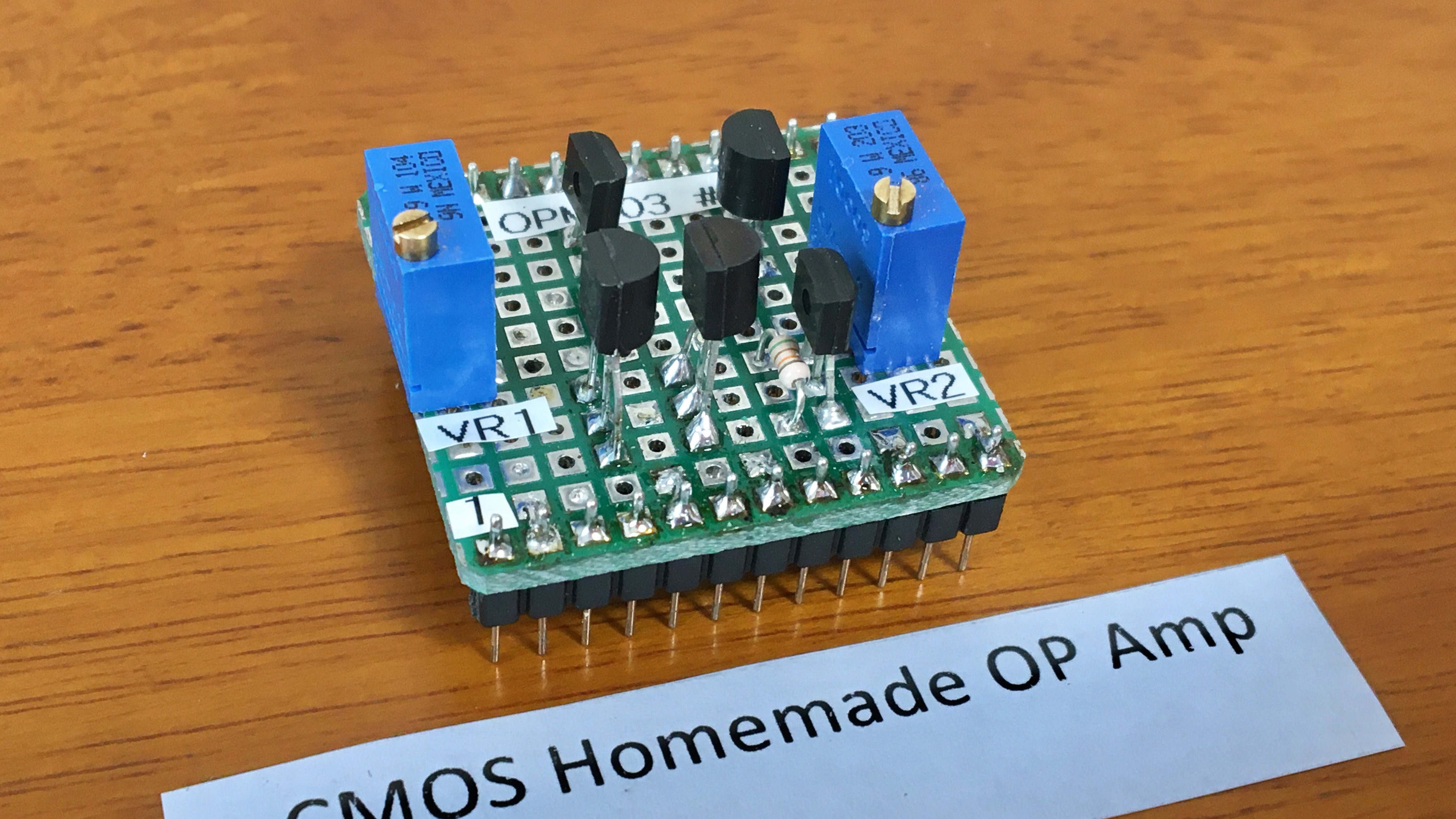
Fig. 2 CMOS simple discrete operational amplifier OPM-03
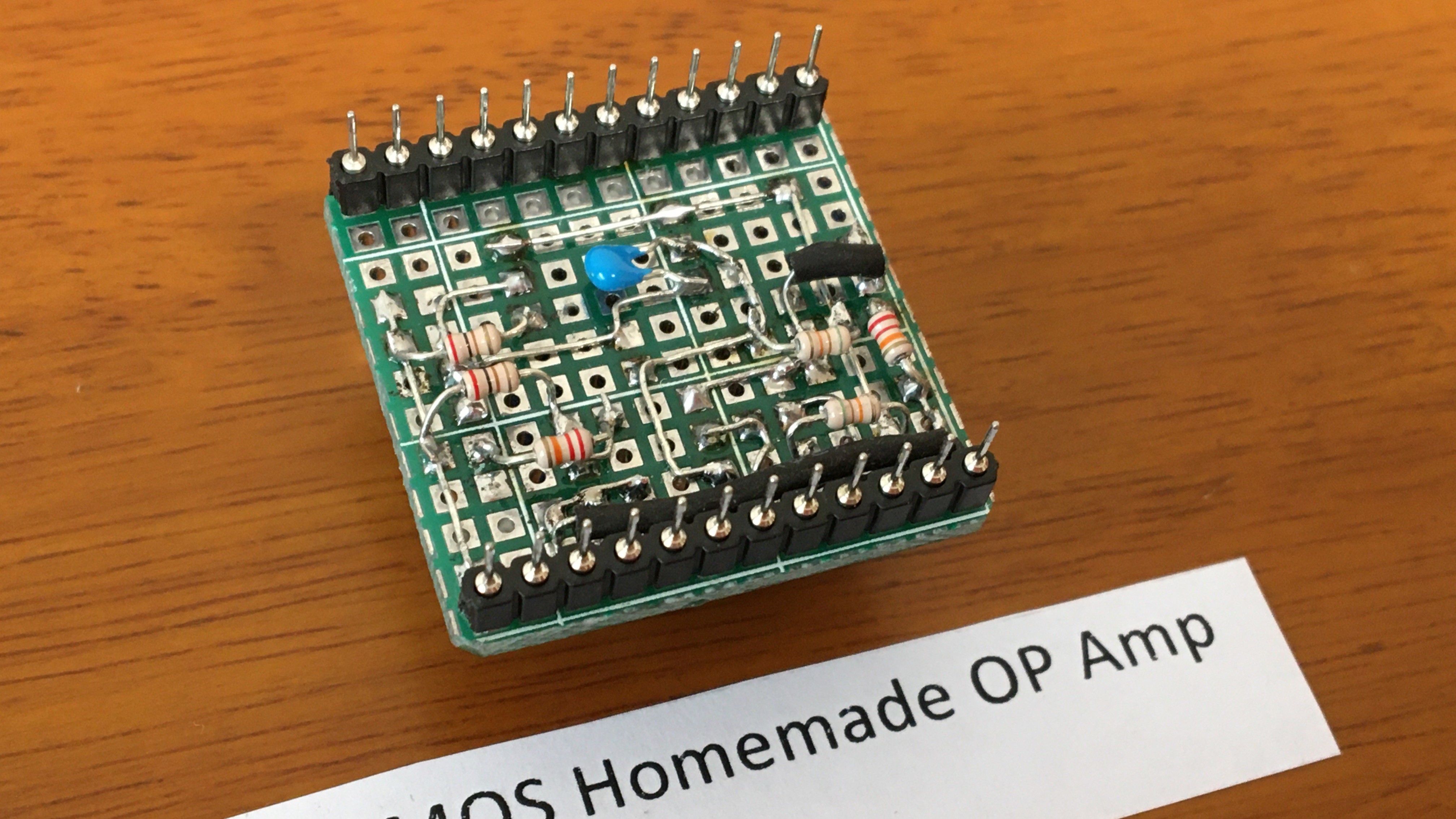
Fig.3 Bottom side of CMOS simple discrete operational amplifier OPM-03
1-2. Differential pair
As shown in Fig. 1, the differential pair consists of TR1 and TR2 N-Channel MOSFETs. The load of the differential pair is the resistors R1 and R2. Typically, a current mirror is used for this load; VR1 and R7 are substitutes for the bias and current sources of a typical differential pair. The drain DC potential of TR1 must be such that the gate potential of the second stage TR3 is operational and the DC offset of the third stage output is zero. It is this VR1 that sets the differential pair operating points so that the drain potential of TR1 satisfies these conditions.
1-3. Gain stage
The gain stage consists only of TR3, a P-Channel MOSFET; C1 is a phase compensation capacitor to prevent parasitic oscillation.VR2, R6 and R3 are the loads of TR3. The potential difference created by VR2 and R6 is to provide a difference in the gate potential of the third stage source follower to eliminate crossover distortion.
1-4. Source follower
The third stage is a complementary source follower with N-channel MOSFET TR4 and P-channel MOSFET TR5. R4 and R5 are simple protection resistors to limit excessive drain current of TR4 or TR5 in case of output short circuit. However, the power rating of these resistors should be about 2 W. The small resistors pictured in Fig. 3 are not correct.
1-5. Evaluation unit
Figure 4 shows the circuit diagram of the evaluation unit for the homemade discrete operational amplifier module. The non-inverting amplifier circuit, open-loop operation, and photo detector operation with transimpedance amplifier configuration are made possible by toggle switches. The gain can be switched with a rotary switch. Figure 5 shows the inside of this evaluation unit.
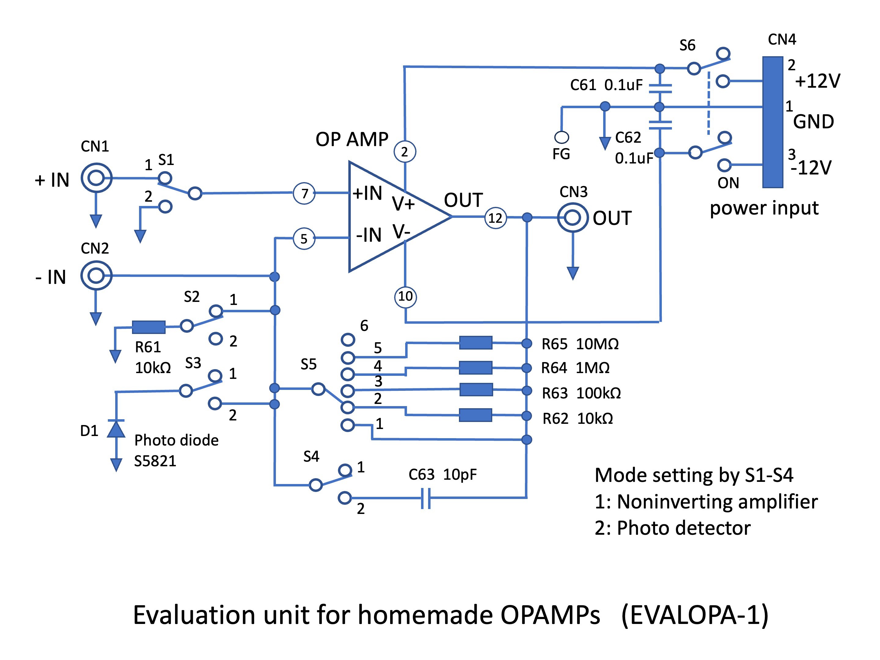
Fig. 4 Evaluation unit for the homemade operational amplifier modules
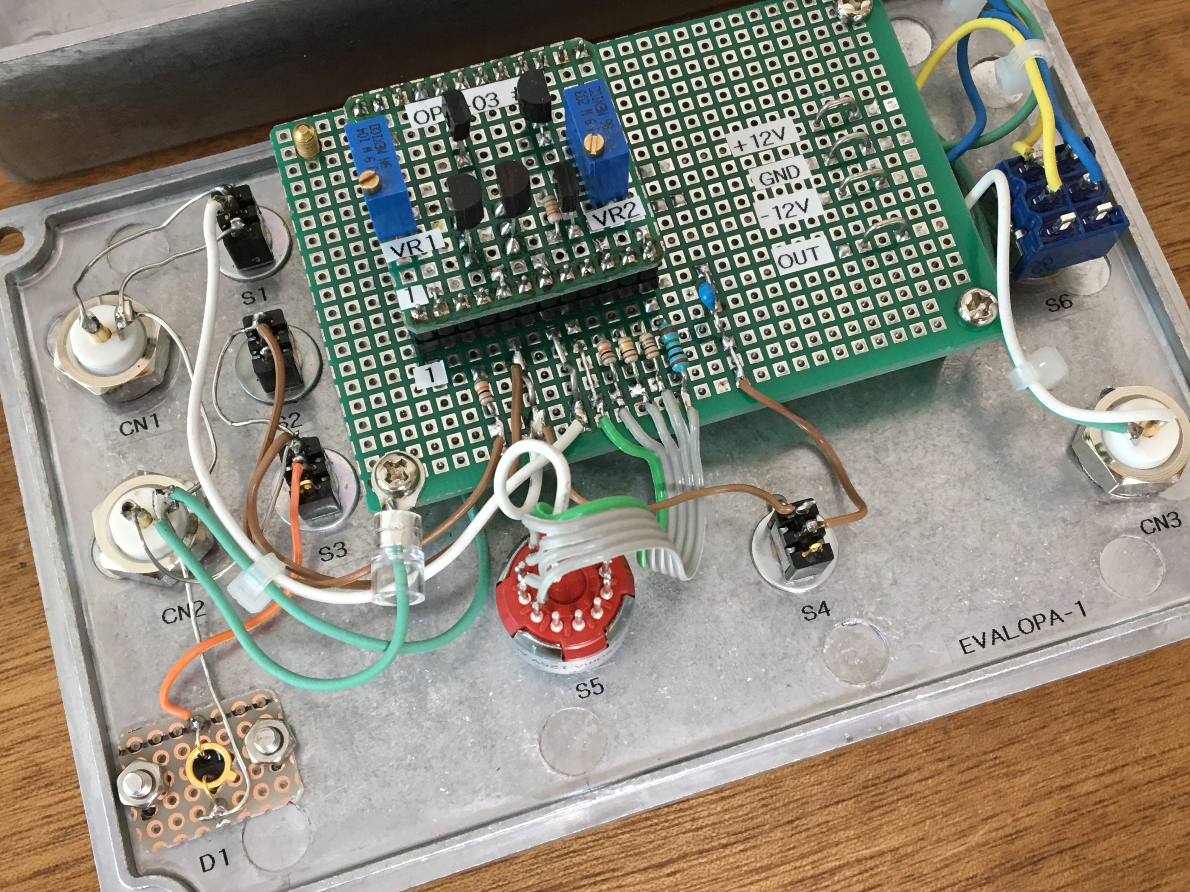
Fig. 5 Inside of the evaluation unit
2. Results
The results of the evaluation of the OPM-03's basic characteristics, non-inverting amplifier, and photodetector operation using this evaluation unit are shown below.
2-1. Result (Operating point)
A typical example of the operating point inside the operational amplifier is 101 kΩ for VR1+R7, +9.01 V for the drain of TR1, and -1.90 V for the source of TR1, under conditions where the supply voltage is +/-12 V and the output offset is 0 V at 0 V input. However, when the FET element was replaced, the value of VR1+R7 at the operating point could be as low as 90 kΩ.
2-2. Result (Input bias current)
The input bias current is less than 10 nA, which was too small to measure with my measuring equipment. In the transimpedance mode evaluation described below, the output offset variation was measured to be 70 uV with a 1 MΩ change in the feedback resistor, so it is estimated that the input bias current would be 70 pA. This is the same as the gate leakage current of a single MOSFET, so naturally it is a good result. In contrast, the OPM-01, which uses bipolar transistors, had an input bias current of about 2 uA.
2-3. Result (Open-loop gain)
The open-loop gain was measured in the non-inverting amplifier configuration shown in Fig. 4 with the feedback resistor selection switch S5 set to open. 2 mVp-p sine wave was input to +IN, and the 3.4 Vp-p output waveform was observed with an oscilloscope. Measured the open-loop gain is 1680x (64.5 dB) shown in Fig. 6 as a solid line. The open-loop gain of the bipolar transistor version OPM-01 in the previous project is shown in this figure as a broken line. Compared to commercially available operational amplifiers, which have an open-loop gain of about 120 dB, OPM-03’s open-loop gain is quite small, so a high gain amplifier configuration would result in a large error.The actual gain error in the 101x gain amplifier configuration was 3%, while the gain error in the 1001x gain amplifier configuration was 65 %.
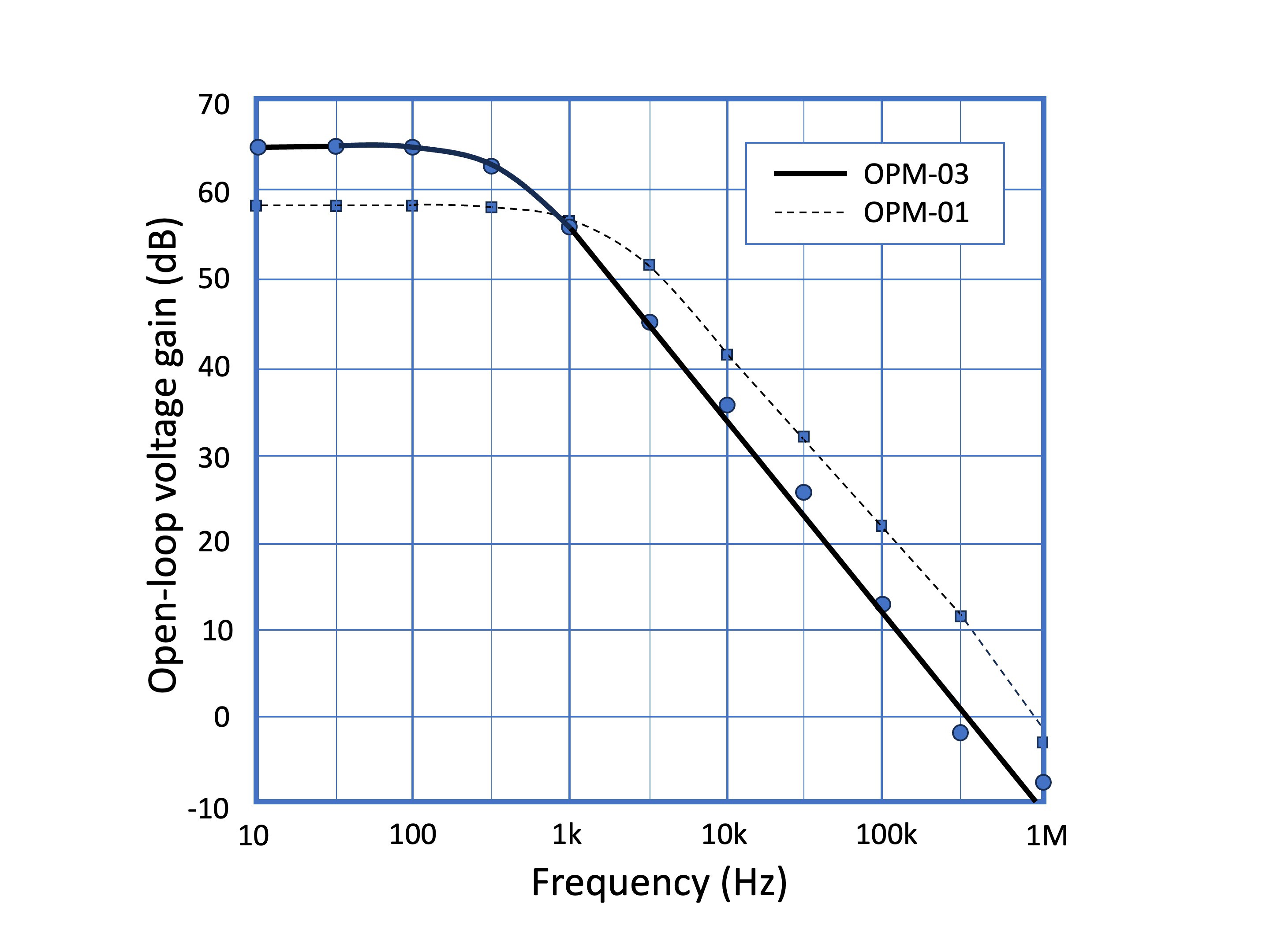
Fig. 6 Frequency response of OPM-03 and OPM-01 for open-loop gain
2-4. Result (Non-inverting amplifier)
Figure 7 shows the operation test of the non-inverting gain 11x amplifier on the evaluation unit. The input signal waveform (1kHz, 200 mVp-p) is displayed on the upper side of the oscilloscope screen (display sensitivity 500 us/div, 500 mV/div) and the output signal waveform (2.22 Vp-p) on the lower side. The theoretical gain at the measured resistors R61=9.872 kΩ and R63=98.52 kΩ is 10.98x, while the measured gain is 11.11x with a gain error of 1.1 %
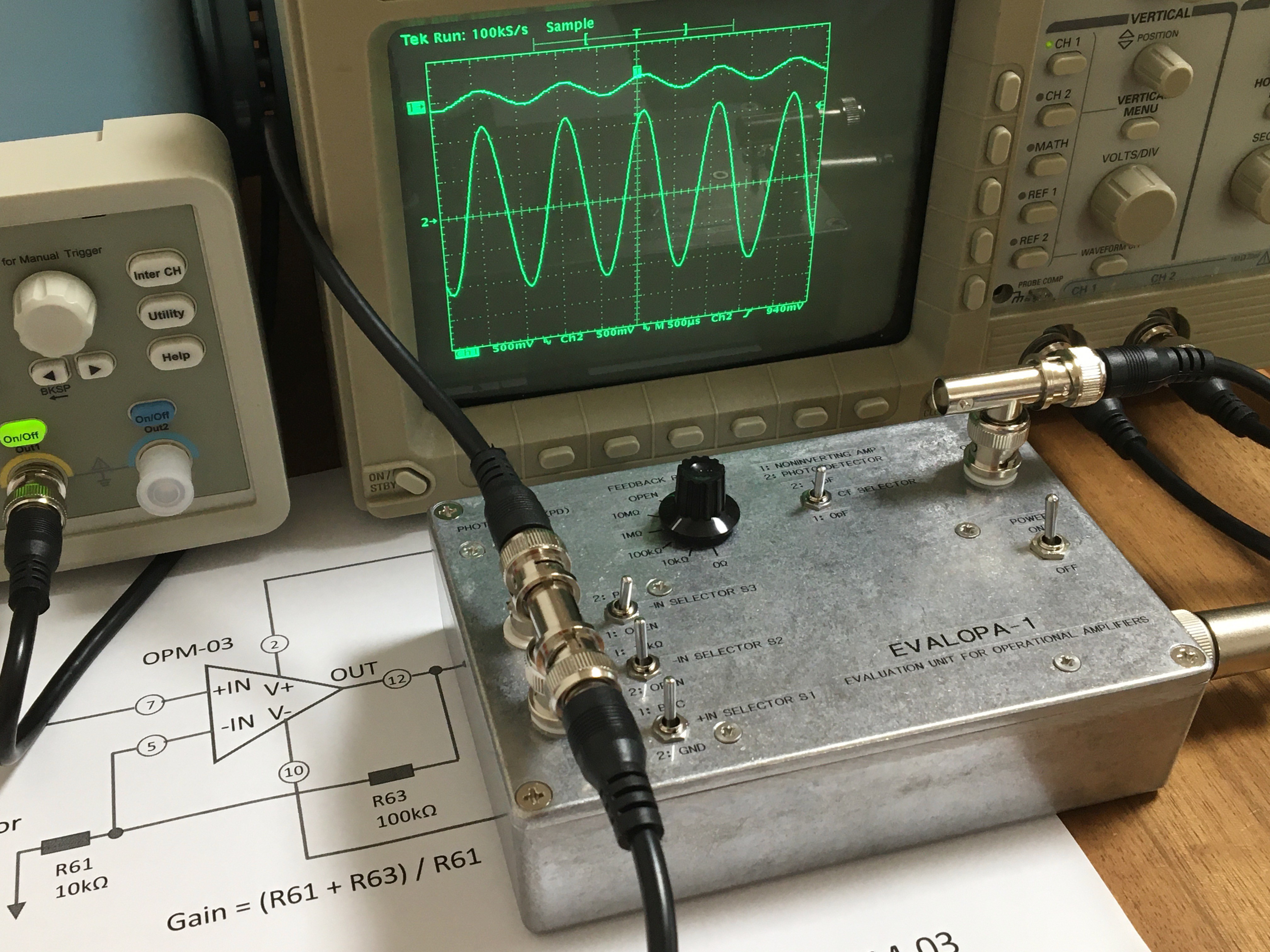
Fig. 7 Evaluating for the non-inverting amplifier with a gain 11x
2-5. Result (Gain Bandwidth Product)
The GBP measurements were also obtained as a result of the input frequency versus gain during the open-loop gain measurements shown in Fig. 6. The obtained GBP is 250 kHz – 400 kHz. It is thought that the GBP can be increased if C1 is made even smaller, but a detailed evaluation is necessary to ensure that parasitic oscillation does not occur.
2-6. Result (Power Supply Rejection Ratio)
The PSRR is sufficient for positive power supply fluctuations at around 70 dB, but is 33 dB for negative power supply fluctuations, in actual measurement. A 1 V change in the negative power supply causes an offset change of 23 mV in input conversion. Since the differential pair is a simple circuit with a simple potential determination mechanism, the PSRR is significant inferior to commercially available operational amplifiers, which have a PSRR of about 70 dB. This is a clear disadvantage of this op-amp.
2-7. Power consumption, operating voltage
The measured power consumption is 7.2 mW (+/-12 V, 0.3 mA) with no input, no load, and minimum VR2. When VR2 is maximum, it is 79 mW (+/-12 V, 3.3 mA). With a supply voltage of +/-12 V, the maximum output voltage is +/-6.4 V with no load, but with a supply voltage of +/-5 V, the maximum output voltage is +/-1.6 V. Due to the large Vth of the MOSFET element used, it is not suitable for very low-voltage operation.
3. Photo detector application by transimpedance amplifier configuration
When the toggle switch S1-S4 is set to the 2 side on the evaluation unit, the circuit becomes a transimpedance amplifier configuration, and a photodiode fixed on the top of the unit is connected to the input. The transimpedance amplifier is a circuit that converts the current input i into a voltage output with the relation V = - i x R. Here, the photodiode is the current source.
3-1. Gain linearity and offset
First, as an evaluation of the steady-state input of the circuit, the operation was evaluated by irradiating the photodiode with light of steady intensity. The measured sensitivity switching error is 3% for switching between 10 kΩ, 100 kΩ, and 1 MΩ feedback resistors to change the conversion gain by a factor of 10, indicating that the transimpedance amplifier is operating almost correctly.
With the photodiode darkened and no optical input, the output fluctuation is measured to be 70 uV even when the feedback resistor is varied from 10 kΩ, 100 kΩ, and 1 MΩ. So, I believe that reproduces the characteristics of a CMOS op amp having a very low bias current. When I tried this with the bipolar transistor version OPM-01, the output offset was as high as 1800 mV with a feedback resistor of 1 MΩ. This shows that an op-amp with a large input bias current is not suitable for a transimpedance amplifier that switches gains.
3-2. Transient response
Next, as an evaluation of the transient response of the circuit, Figure 8 shows the state in which the illumination intensity of the LED light irradiating on the photodiode is switched to weak mode. The output of the transimpedance amplifier is displayed on the oscilloscope, and it can be seen that the light intensity is behaving in such a way that the brightness appears to be weakened by the pulse density, which repeats light and dark at a 260 us period. The output signal rises at a rate of 12 us/ 1 V. It would be possible to observe the light intensity changing at several 10 kHz with this configuration.
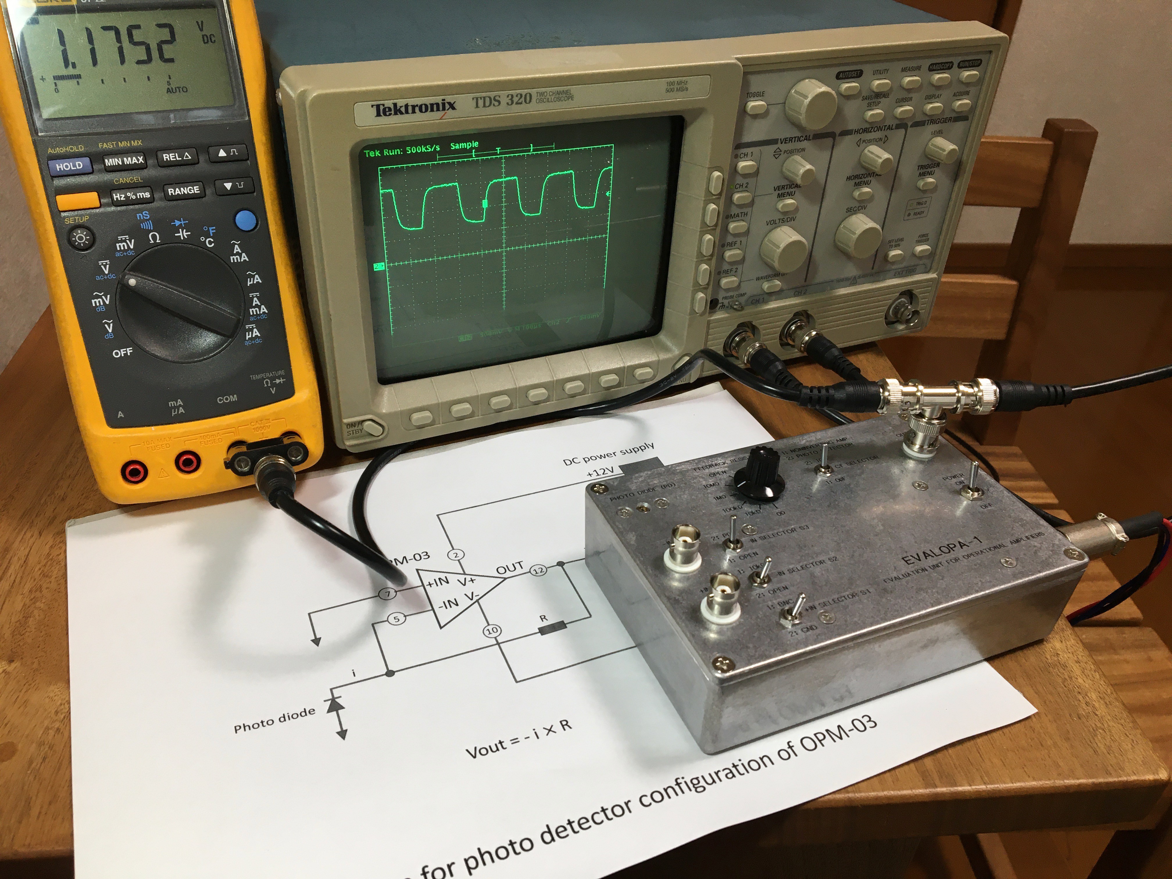
Fig. 8 Evaluating for the photo detector circuit with transimpedance amplifier configuration
4. Summary
Video 1 in the following shows an evaluating of the CMOS homemade op-amp OPM-03. There is no audio explanation, so please turn on the subtitles to watch.
Video 1 Evaluating of the CMOS homemade op-amp OPM-03
This time, I was able to deepen my understanding of the characteristics of CMOS op-amps by building homemade simple CMOS op-amp with a discrete circuit and measuring its operation. Table 1 shows a comparison of the measured characteristic values of OPM-03, and OPM-01 which is a bipolar transistor version previous project.
Table 1 Comparison of OPM-03 and OPM-01
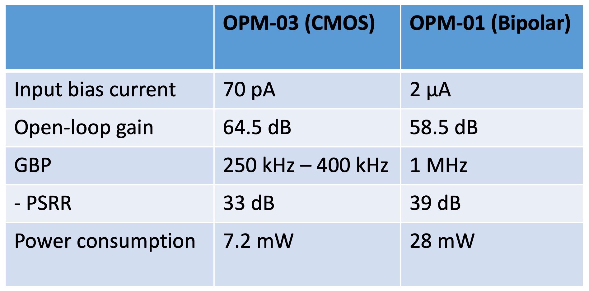
The extremely small input bias current characteristics of CMOS operational amplifiers are reproduced adequately shown in Table 1. The evaluation also well demonstrated that a transimpedance amplifier with a large conversion gain for photodetectors requires an op-amp with an extremely low input bias current. Note that the OPM-01 circuit require further consider, but is shown with the circuit characteristics at the time of initial post.
In addition to the above, I was also able to realize that replacing individual MOSFET elements can significantly change the operating point. In this respect, I thought that the variation of Vth in commercially available monolithic ICs would be well controlled by the design and manufacturing process. Although linear CMOS analog circuits were somewhat more difficult for me than circuits using bipolar devices, I am glad that I took on this challenge.
(Posted on May. 17, 2023)
(Latest revision on May. 29, 2023)