 Evangelos Petrongonas
Hello everybody and sorry for the absence, but it is exam period in
the University so I didn’t have a lot of free time. First of all as
you may have noticed in my twitter account the PCB is almost
completed, and in the next week or so, the first prototype PCB’s,
will be ordered :)
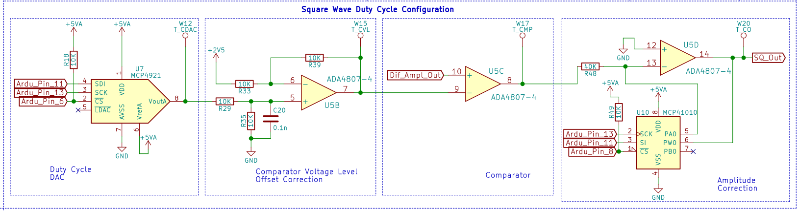
Now let's get into this DesBlog’s topic, which is all about Square Waves and Duty Cycle. Square Waves with variable DC (DC=Duty Cycle), are very important signals in Electronics, as they can be used as clock signals, PWM modulation and many more. The main IC supports Square Wave Creation, using a comparator, which can function in two ways. It can either output the DAC MSB (if the MSB of the 14 bit DAC out value is 1 then it will output HIGH and if it is a zero it will output LOW), or the clock edge, which means that it will output a signal, which very much resembles the input clock. However, creating Square Waves this way is quite limiting, as its is complicated to adjust the frequency and almost impossible to change the Duty Cycle. A workaround for this is to load the appropriate pattern into the AD9102’s SRAM. This is not the optimal way to do it, though especially for such an important feature like the Square Wave Generation. For these reasons I have opted for a hardware implementation, which is shown down below.
Well it might not be that obvious how it works in first glance, but
it is pretty simple. First of all let's look at the basic concept.
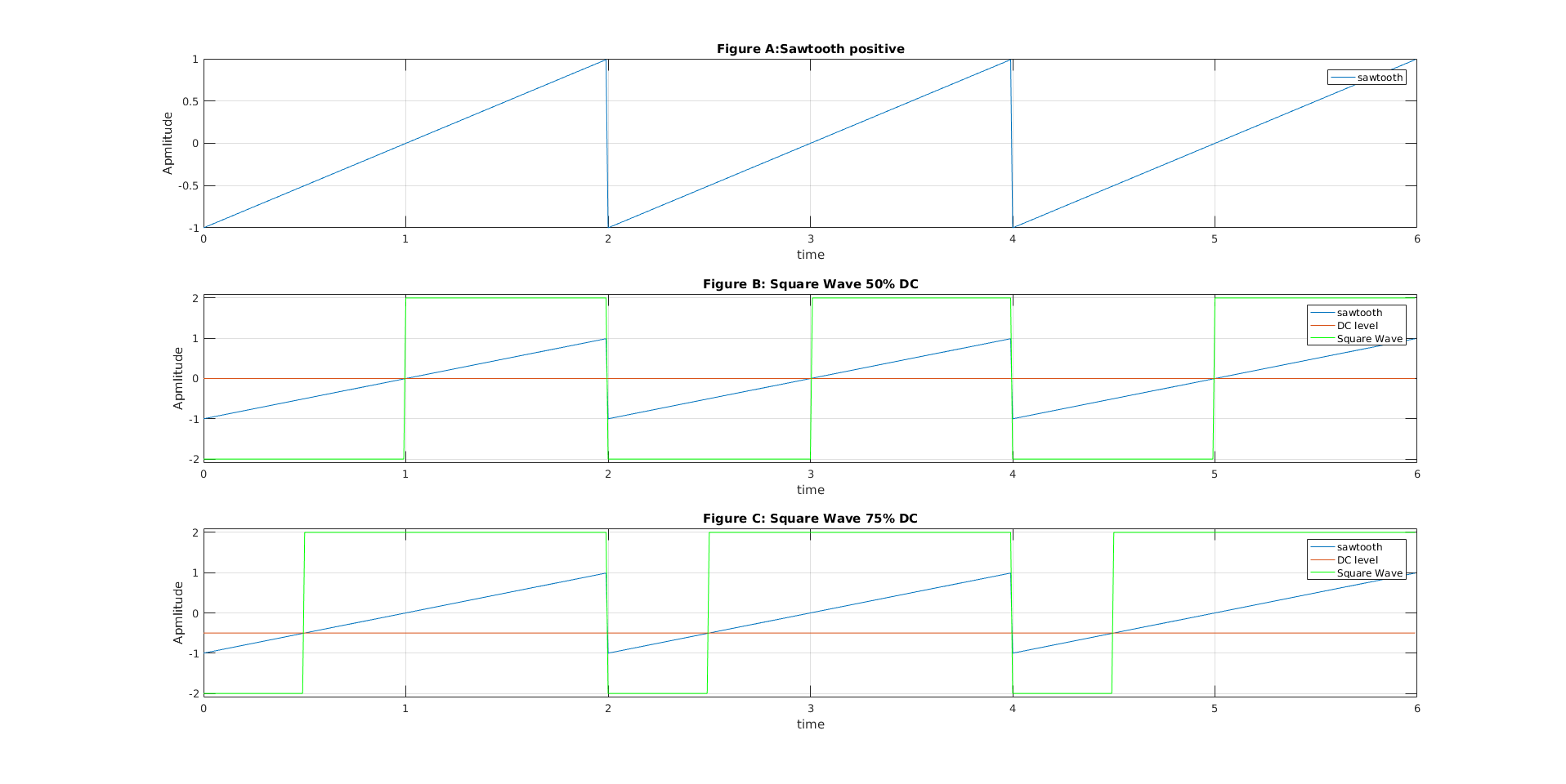
The IC’s DDS will generate a positive Sawtooth as shown in figure
A. This signal is fed into an Op Amp which acts as a comparator. The
other Input is DC Voltage level. When the input signal value is
higher than the DC level, then the OpAmp output will jump to
Positive Voltage saturation level, in this case +5V and when it is
lower it will output -5 V, which is the negative Voltage Saturation
value. So by changing the DC Voltage level, the Duty Cycle can be
adjusted as shown in figures B and C. As far the frequency is
concerned this can be configured by the sawtooth frequency. Bear in mind that the axes are arbitrary and do not correspond to a real vale
The other Op Amps and IC’s are auxiliary and their function is the
following. The input signal coming from the AD9102 is AC coupled
which means there is no DC offset and the mean value is zero. In
order for the comparator to work, the DC level must take both
positive and negative values. This is done using a DAC (U7-MCP4921),
in order to create a precise DC voltage in the range of 0-5Volts.
Afterwards it is fed into the non inverting input of the OpAmp. The
inverting input is a 2.5 Volt reference and the opAmp is in a unity
gain Differential topology. This configuration is used also for the
output offset generation so it will be covered in more detail in a
future DesBlog, but for now just to give you an overview when the DAC
output is 0 then the Voltage Level will be -2.5 V and when the output
is 5Volts, the voltage level will be 2.5 V. This is the drawback
mentioned in the previous DesBlog, caused by the Signal Generation
Opamps.
Last but not least the Amplitude must be configurable, as the comparator output will output a 10 Vpp signal. This is done with the help of an opAmp which is in simple Inverting configuration, but the feedback register is implemented using a digital potentiometer (U10-MCP41010) in order to set the wanted gain (which is less than one, as we want to decrease the Amplitude), just like we did back in DesBlog #1.
That’s all for today’s DesBlog and as always I’ll be more than happy to hear your thoughts and suggestions.
See you all next time :)
Discussions
Become a Hackaday.io Member
Create an account to leave a comment. Already have an account? Log In.