 Evangelos Petrongonas
elcome back everybody, the ArduGen Schematics are, hopefully,
completed and most probably only minor tweaks will change in the
design from now on. However, I do not want to publish a design which,
will be scrapped eventually, so instead of releasing the schematics
all at once, I’ll reveal it in small steps in each DesBlog.
This time we’ll talk about the Signal Generation Op Amps. As you can see in the schematic below, this module consists of three Op Amps, the function of which, will be explained down below.
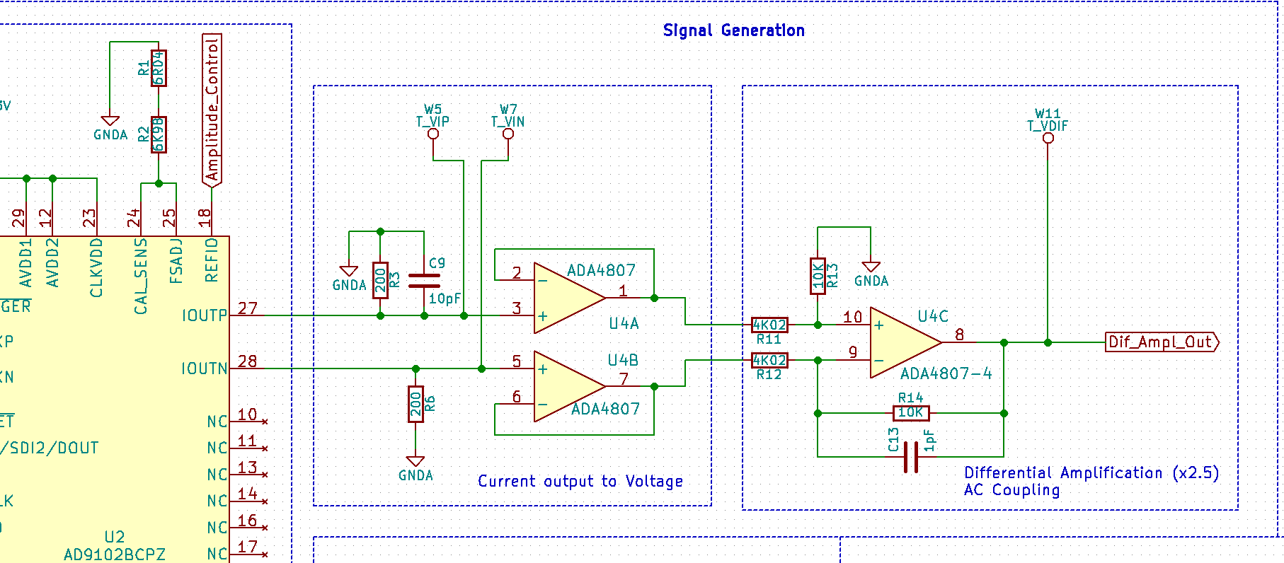
For the time being, please ignore the Main IC which is an AD9102 Waveform Generator, as it is the heart of the design and requires a Log of its own. Before we proceed, though, the following must be mentioned. The AD9102 has a differential current driven output, and in its current configuration, it outputs a maximum current of 5 mA. (more details in a future DesBlog).
The vast majority of Waveform Generators, output Voltage signals and this one is no exemption, so our first task is to transform the current output into a voltage output. This is done by using the 200 Ohm Resistors. As practically, no current flows into the OpAmp inputs, the Voltage across the resistors is 1 V for a current of 5 mA. IN order to ensure accuracy, the signal is buffered using two OpAmps in a voltage follower (buffer) configuration. The now buffered signal, is ready to be amplified. Both the positive and negative current signals (Beware negative doesn’t mean I<0, it means In= Imax-Ivalue), are fed into the non inverting and inverting inputs of the Amplifier, respectively, which is in Differential Amplification topology, with a transfer function of
.The above equations is not exactly true as, i have not taken into account the Capacitor in parallel with Rf. However this may not be in the final design, and will be used only if the first tests show a high frequency noise. Even if it is used however, it will act as a Low-Pass active filter, with the same Amplification ratio as above. Moreover, due to the differential, amplification, the
signal is AC coupled, as the common DC offset is removed, so there is
no need for an external AC coupling Capacitor. This is mostly a good
thing, but it has a downside, which will be made obvious in a future
DesBlog.
A question now arises, why the amplification is only 2.5 times instead of 5, as it is shown in the Specs (5Vpp Output). The answer to this question lies in the GBW vs Frequency Curve, a diagram of the maximum amplification of the OpAmp, in the various frequencies. Higher Frequency equals to lower Amplification ratio, so to avoid Amplification distortions, the amplification will happen in two stages.
One last note, for those who have read the previous DesBlog, as you can see the OpAmp used now, is the ADA4807-4 a 4 channel IC, which is better than the LM6142, in almost every aspect, especially as far as the GBW and the SR are concerned, while maintaining very low power consumption.
See you all in the next DesBlog, where we will take a look at the square wave, Duty Cycle and Pulse Generation Module :)
Discussions
Become a Hackaday.io Member
Create an account to leave a comment. Already have an account? Log In.