 Frédéric Druppel
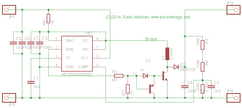
As said in the project details, I based my schematic on the one on this website (link). Here's the said schematic, so you don't have to leave this page ;)
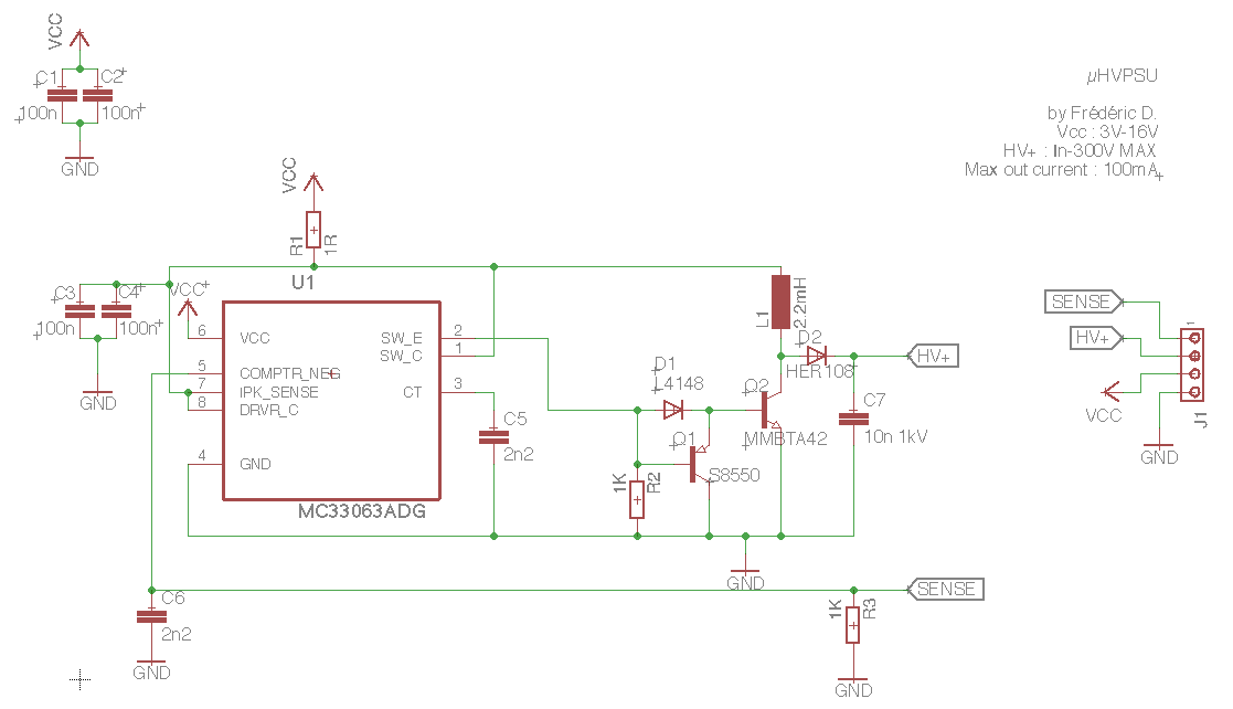
 However, I changed a few things in my design.
First of all, I used classic 4pin-connector_type-breadboard-friendly-type-thingy to interface the module, so it is easier to implement in other designs.
Secondly, I changed the feedback loop system. In the schematic above, there are fixed resistors, which give the module a fixed (theoretical) output voltage of approx. 370VDC. In my design there is an interface pin where you put a resistor between that pin and the HV output, so you can always control the output voltage.
Oh BTW, here's the formula to calculate the output voltage (found on the MC34063 datasheet)
In my design (I hate saying that, but anyway) R1 is has a fixed value of 1k. You can choose the value of R2 by putting a resistor between the "HV+" pin and the "Sense" pin.
Here's my version :
All the files can be found in the "Files" tab of the project.
Discussions
Become a Hackaday.io Member
Create an account to leave a comment. Already have an account? Log In.
That driver is designed for MOSFET. For driving a BJT (Q2), you'll need a series resistor for the base to limit the drive current.
Are you sure? yes | no
I know, but the voltage drop of the diode is enough in this application (at least it's what I saw in the tests ^^). There will not be much current flowing trough this transistor.
Are you sure? yes | no