 Ted Yapo
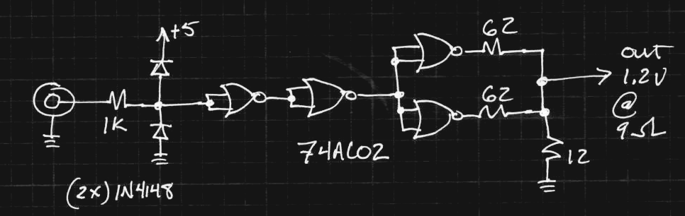
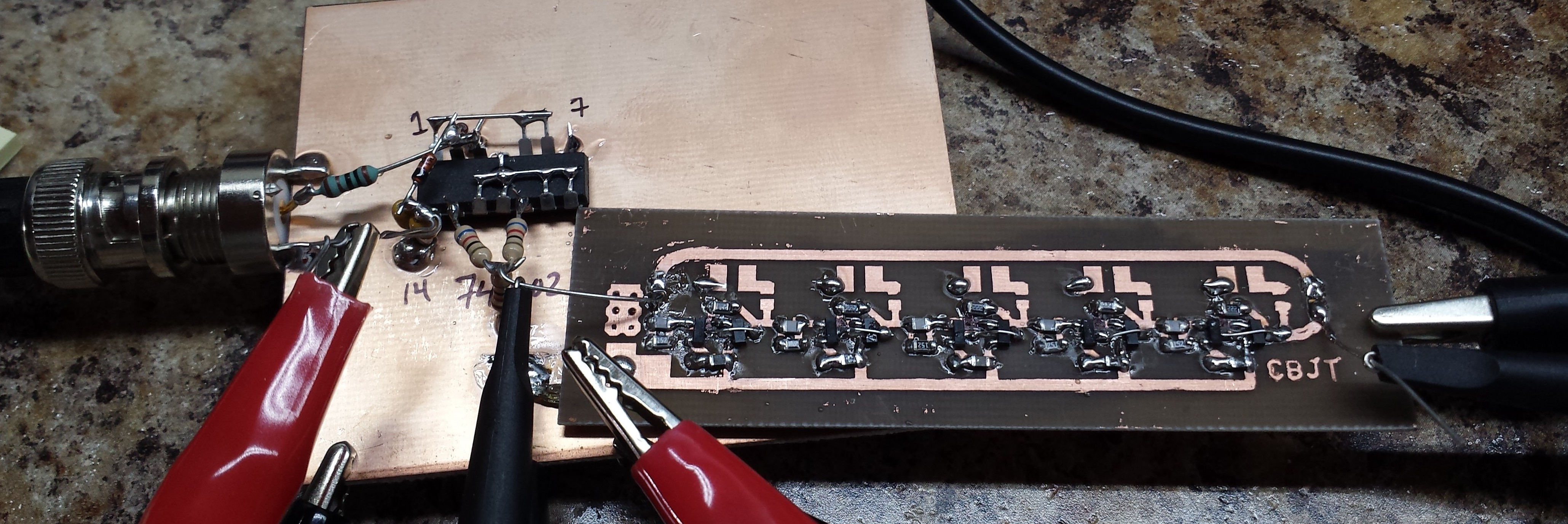
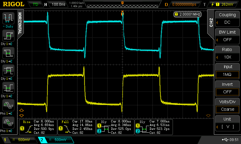
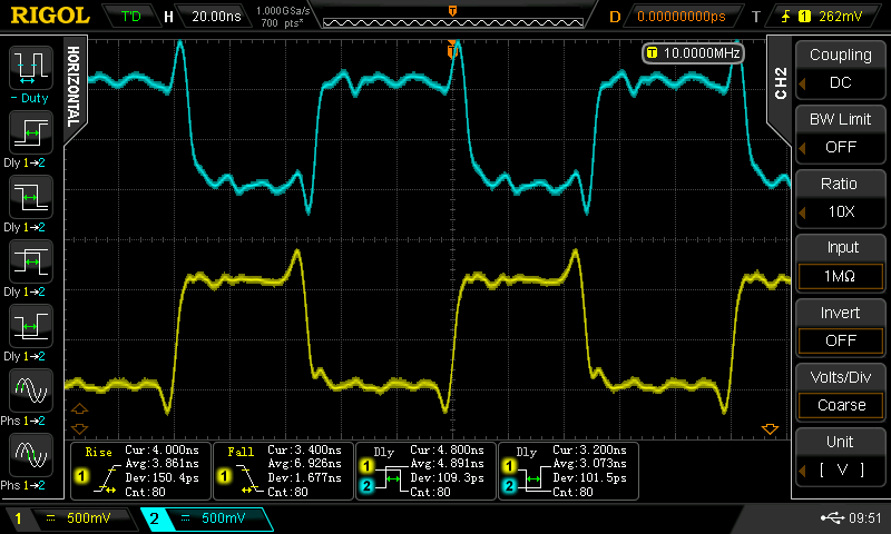
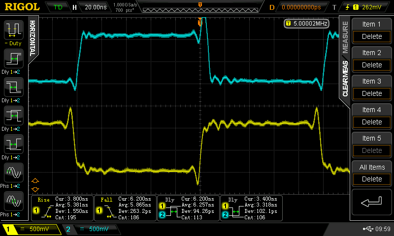
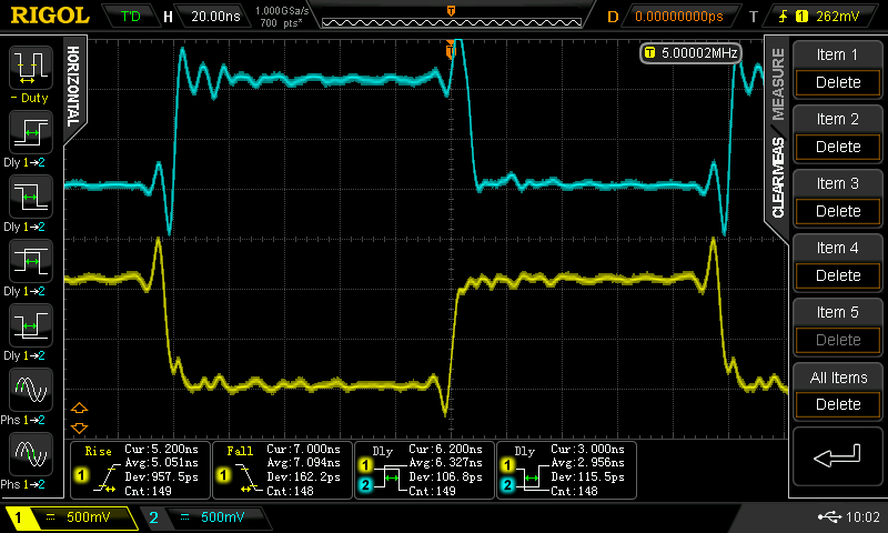
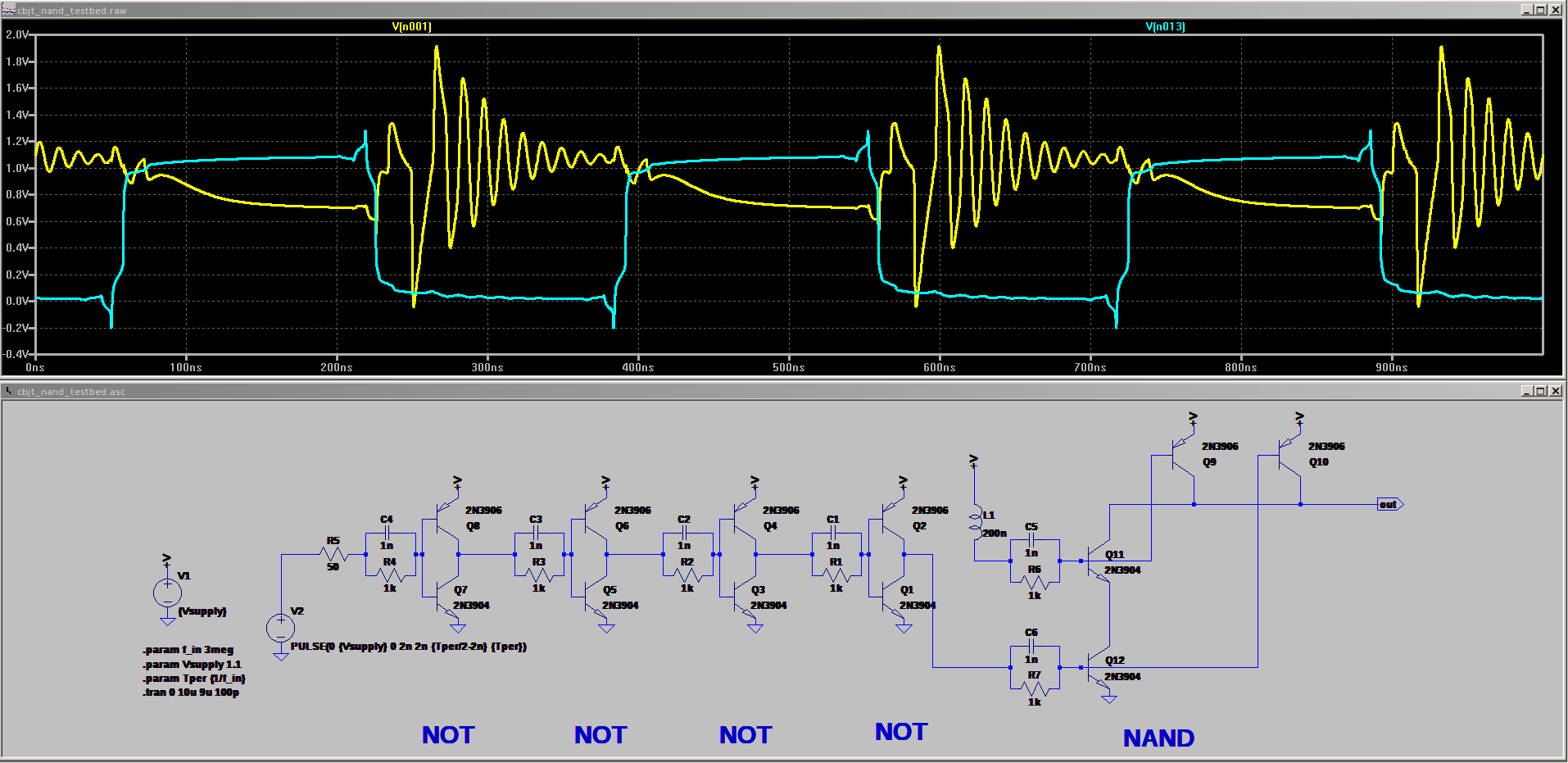
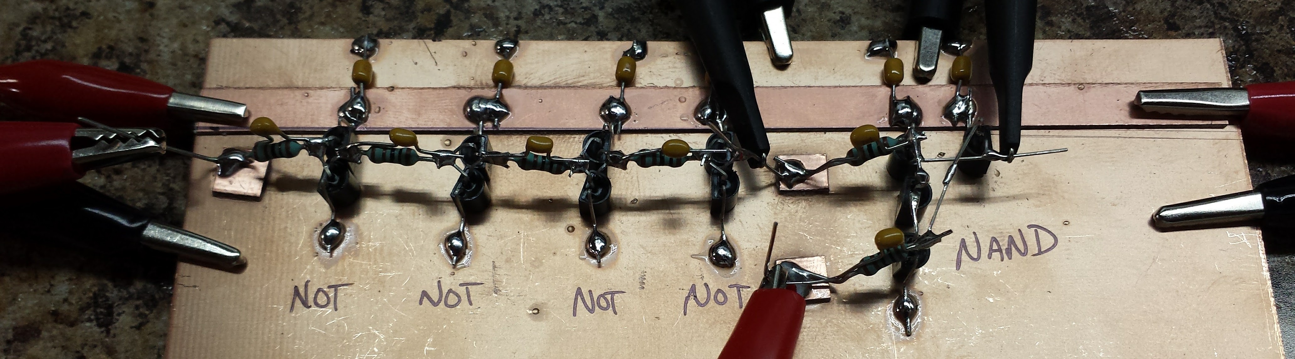
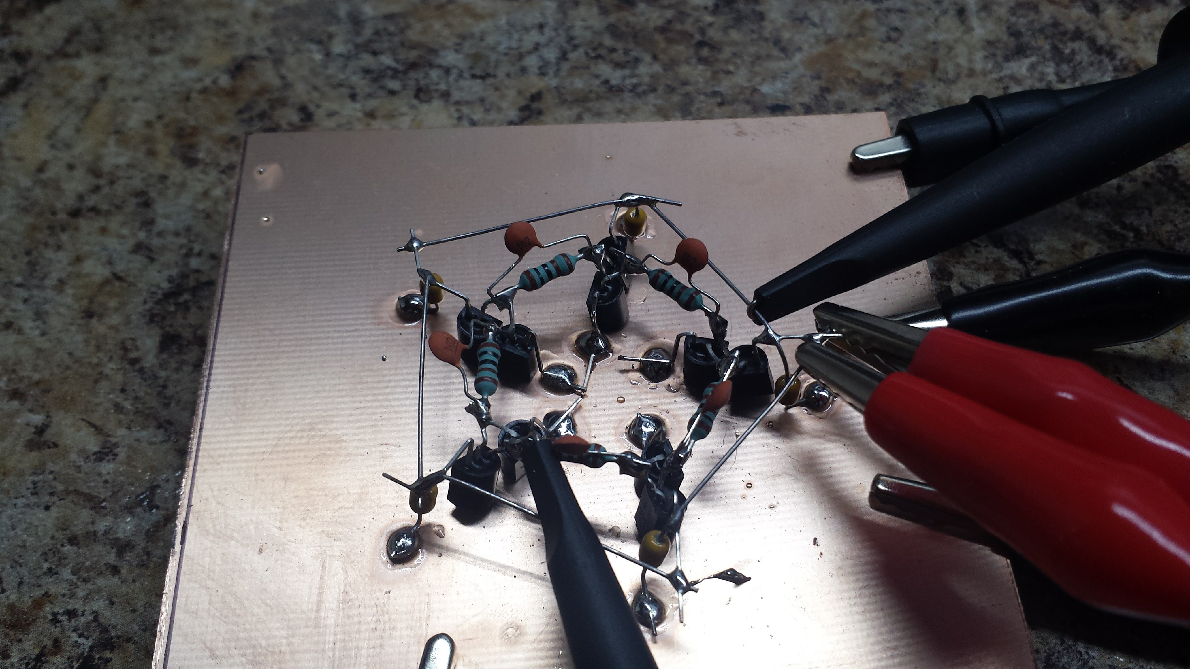
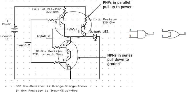
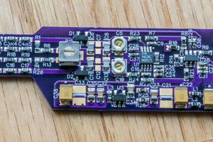
The idea comes from a simple mistake that apparently I was not the only one to make. About 20 years ago, I decided to design a discrete audio amplifier. Not having thought about it for a while before that, I got confused about the emitter-follower output, and made something like this:
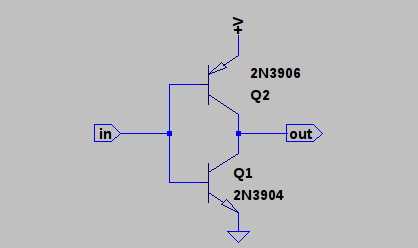
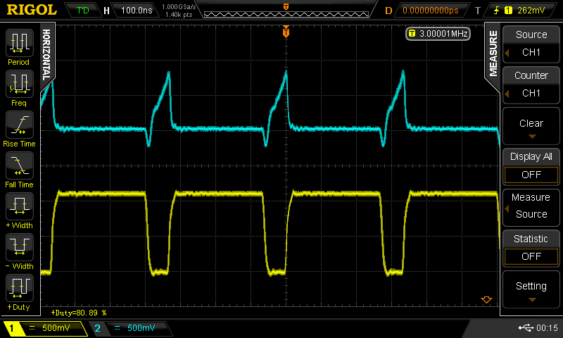
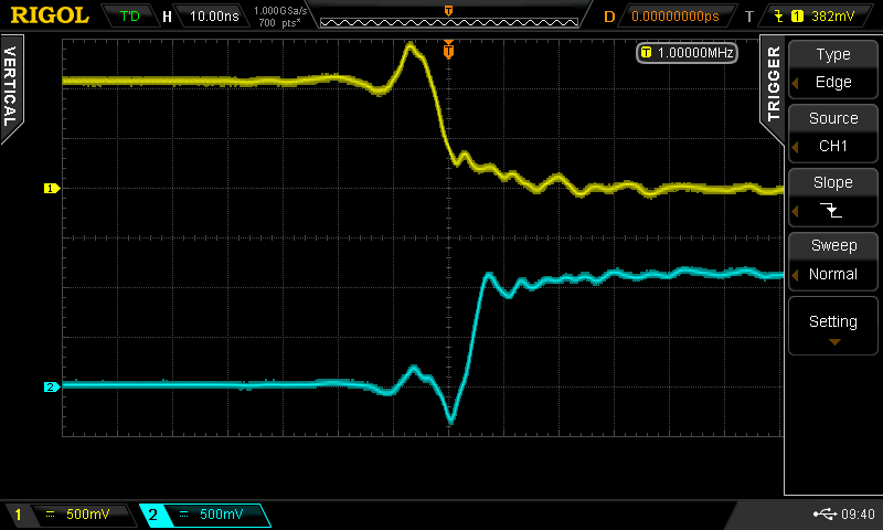
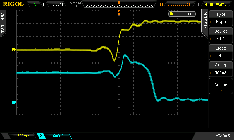
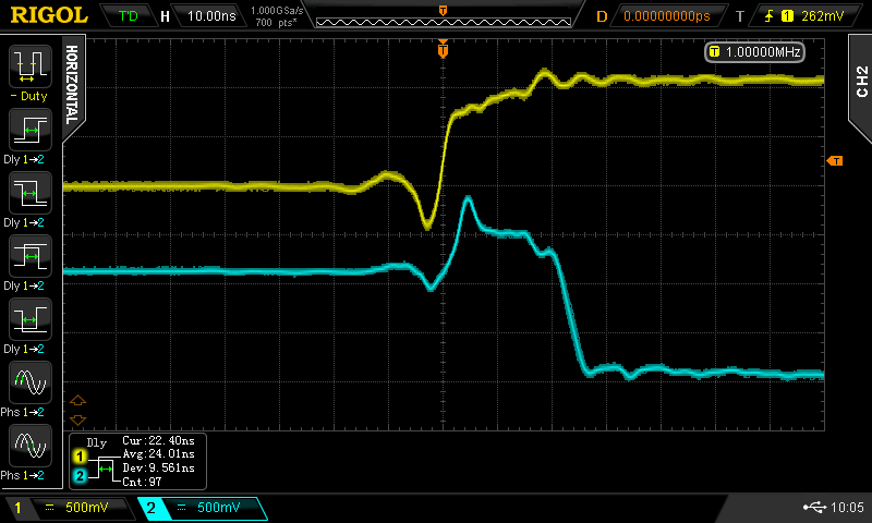
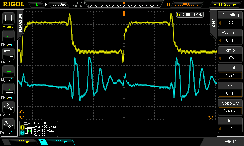
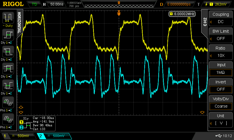
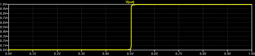
At first, I couldn't figure out why the transistors got so hot. A co-worker who had previously designed audio amps for a boutique audio house pointed out that I had the transistors reversed; these were common emitter switches, not followers. In this configuration, once the supply voltage exceeds about 2*Vbe, the transistors bias each other on and draw lots of current. @esot.eric mentioned a similar learning experience regarding an H-bridge design from around the same time period :-)
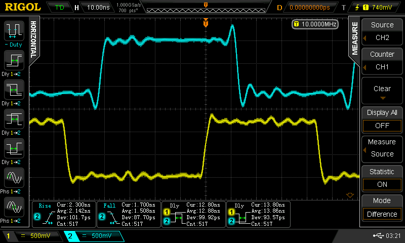
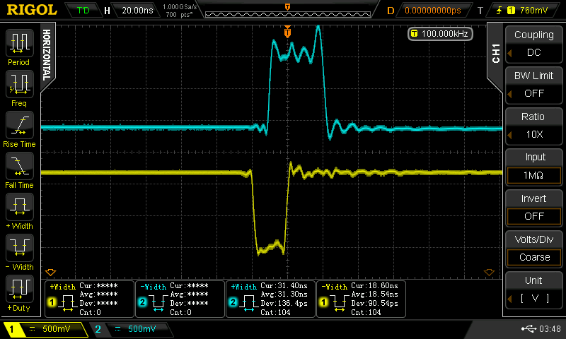
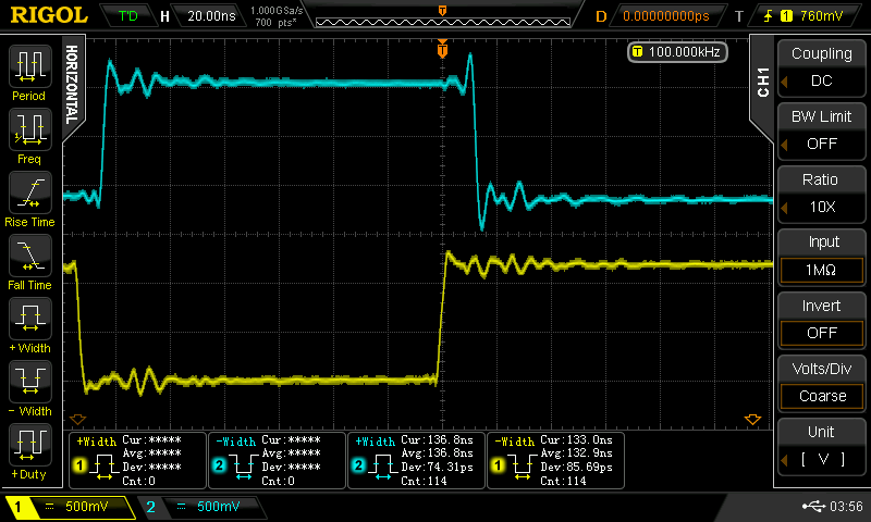
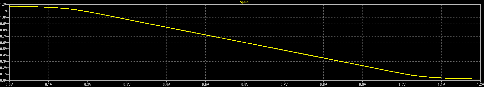
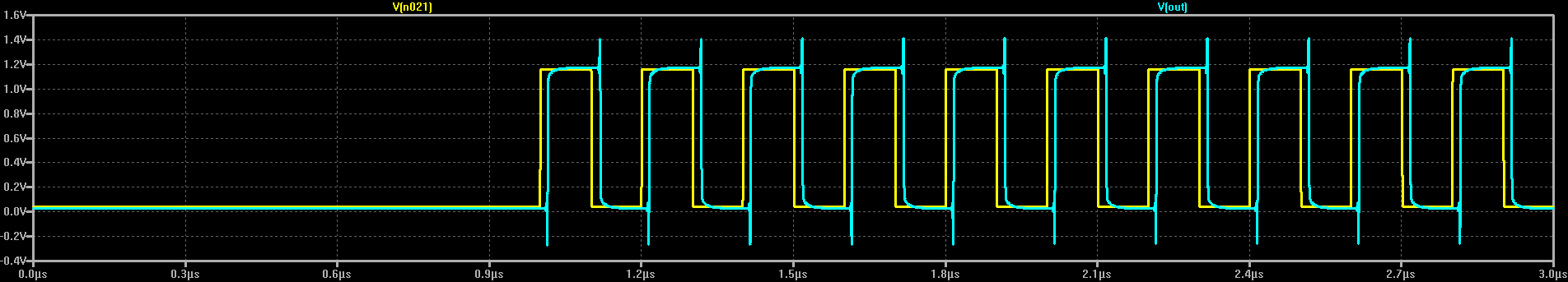
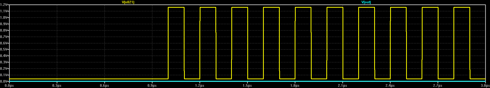
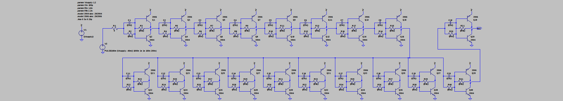
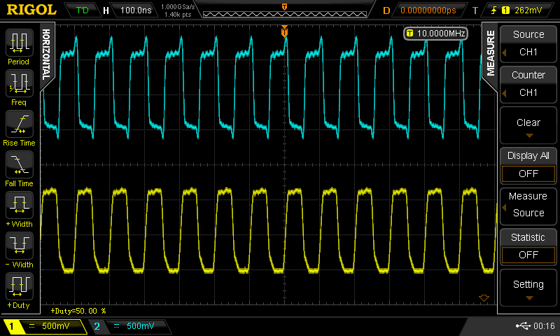
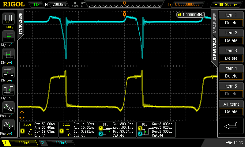
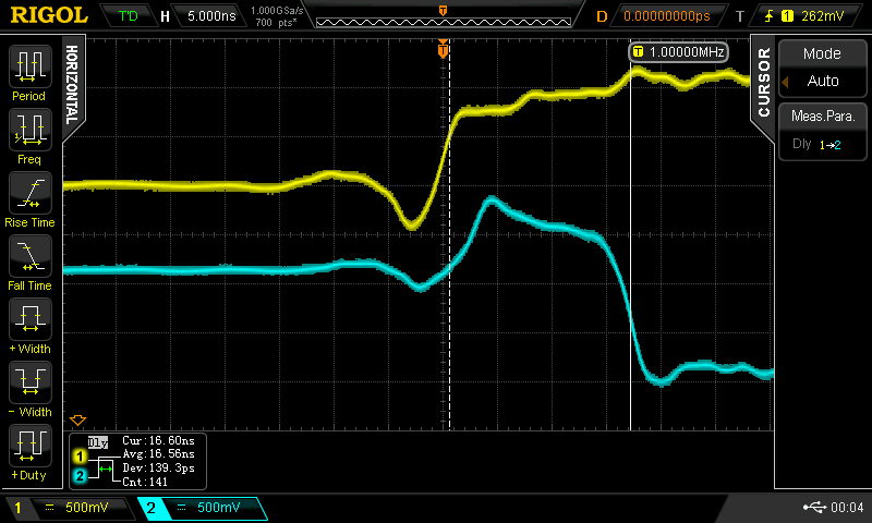
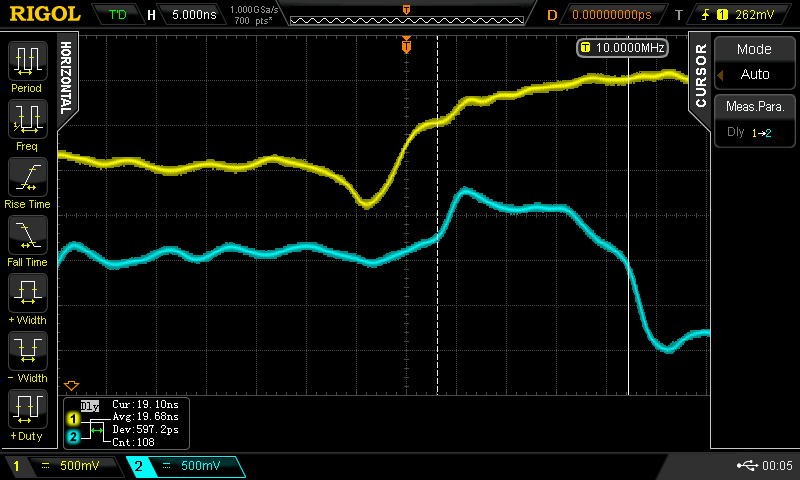
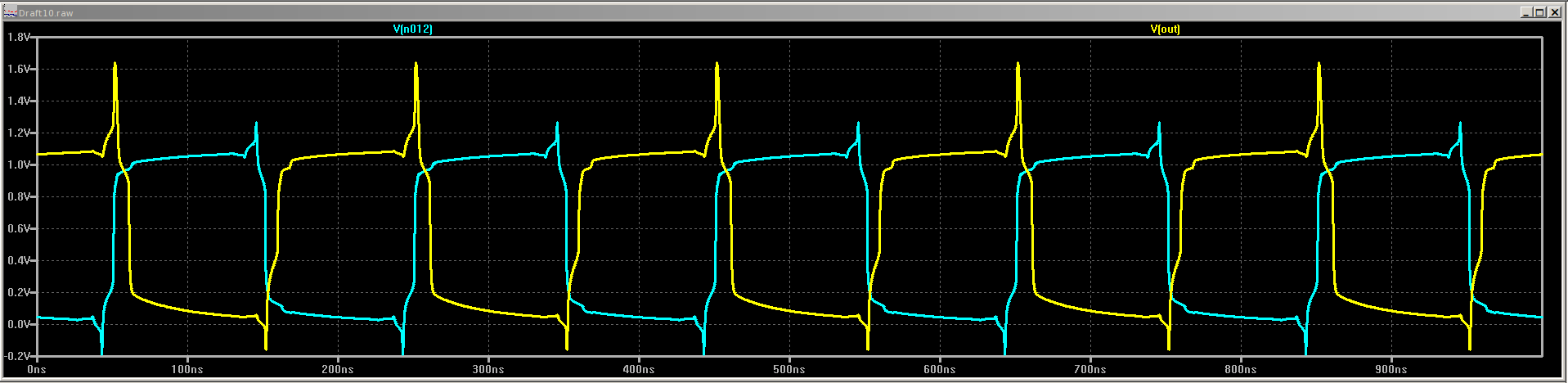
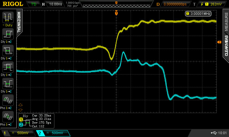
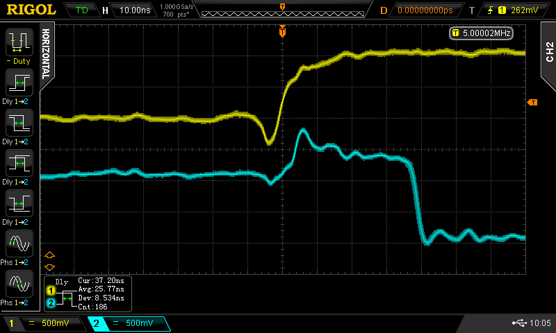
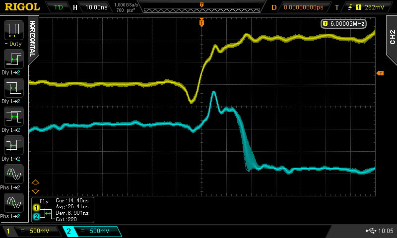
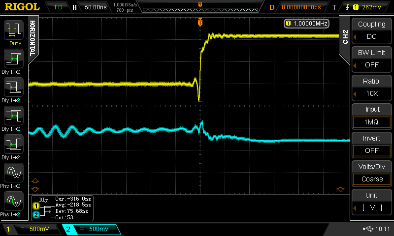
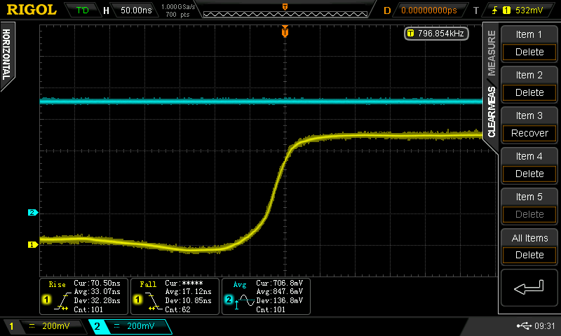
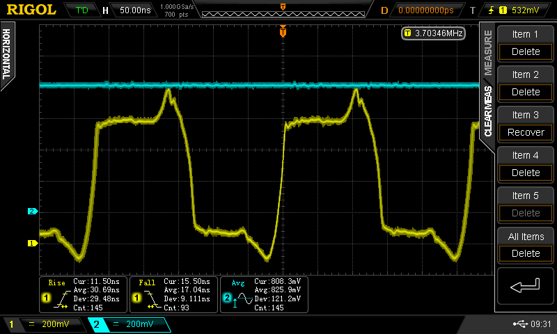
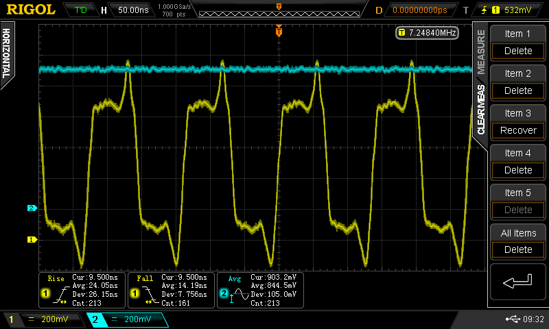
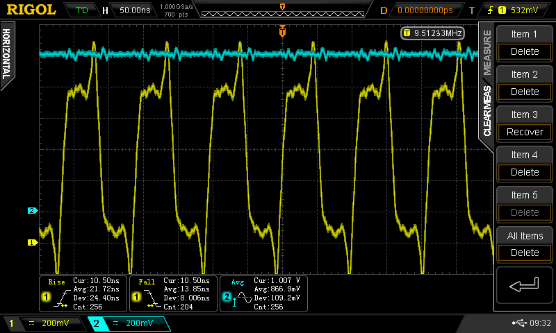
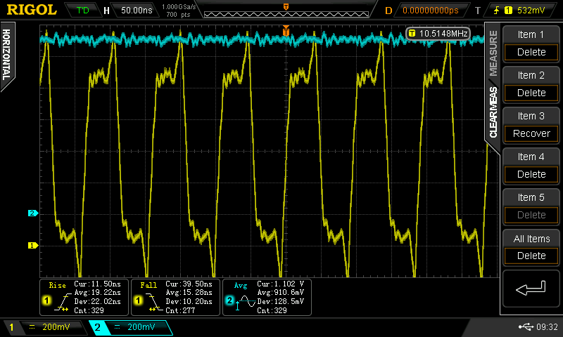
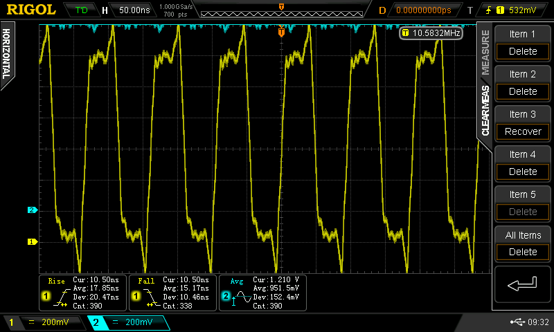
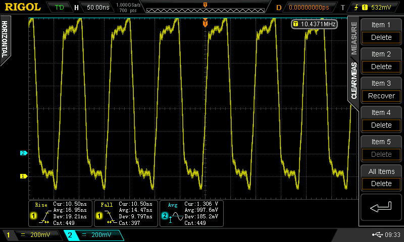
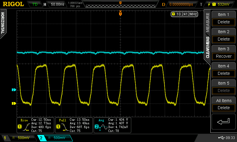
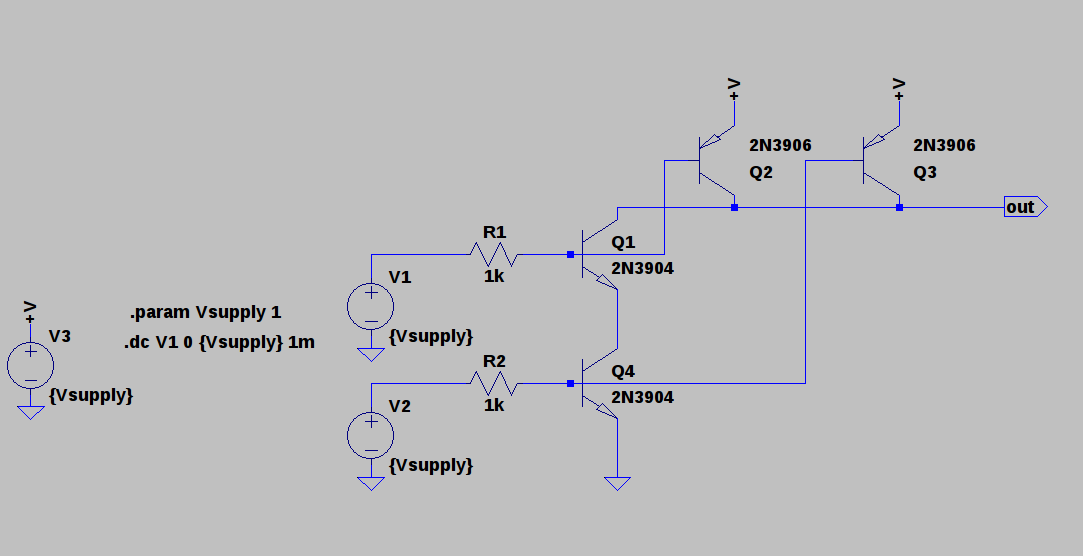
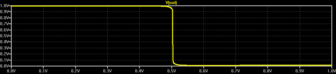
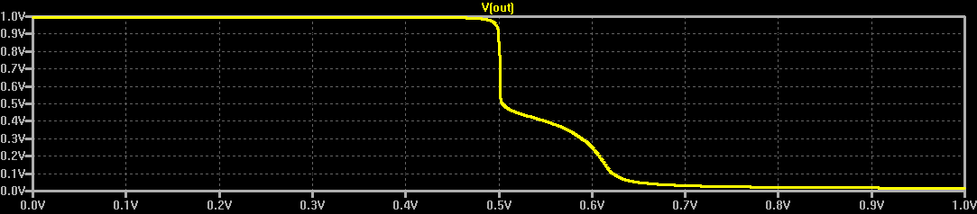
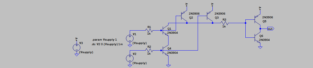
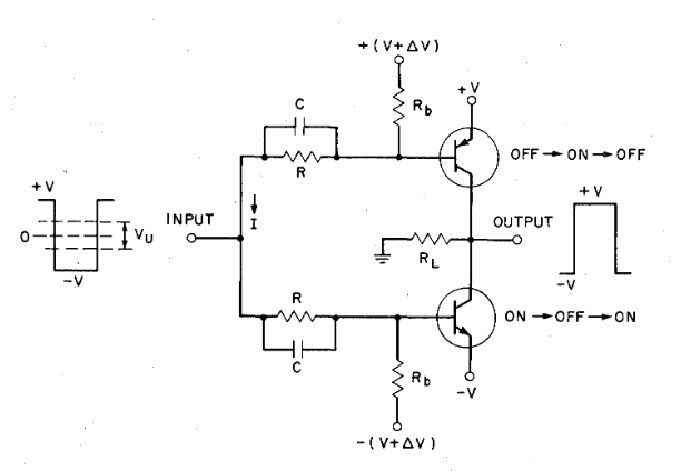
At some point, I wondered what happens with supply voltages less than 2*Vbe - then, the circuit looks a lot like the classic CMOS inverter. I didn't do anything with it at the time, but the subject of unusual transistor circuits recently came up in another thread. It seems like there's enough interest to make this into an actual project...so here goes.
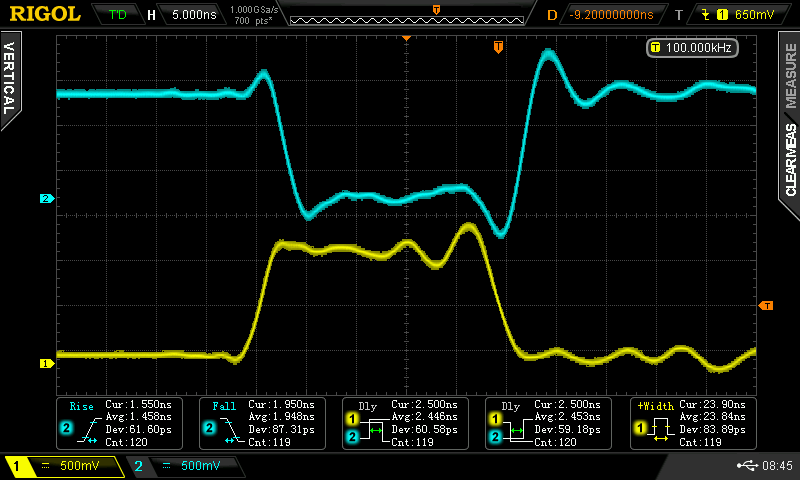
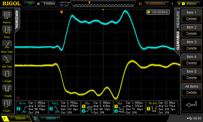


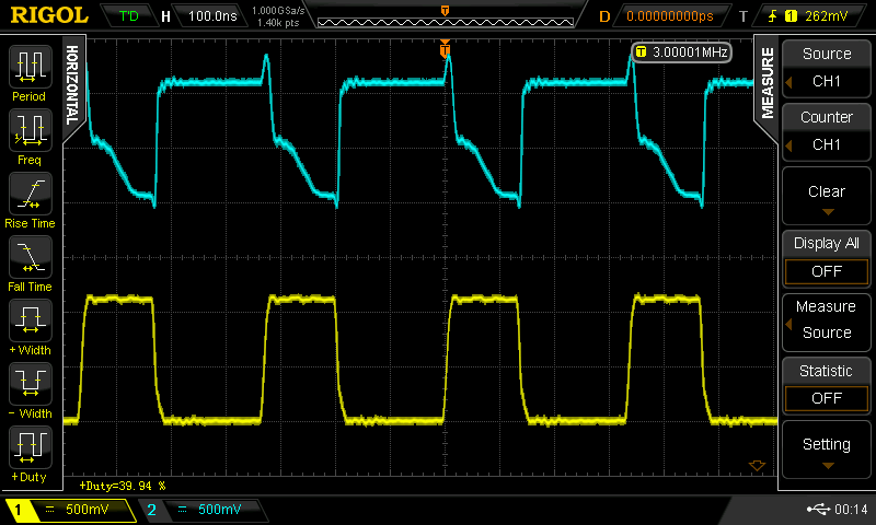
 30%
30%
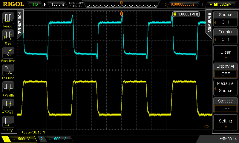
 40%
40%
 50%
50%
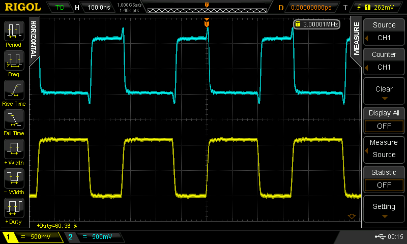 60%
60%
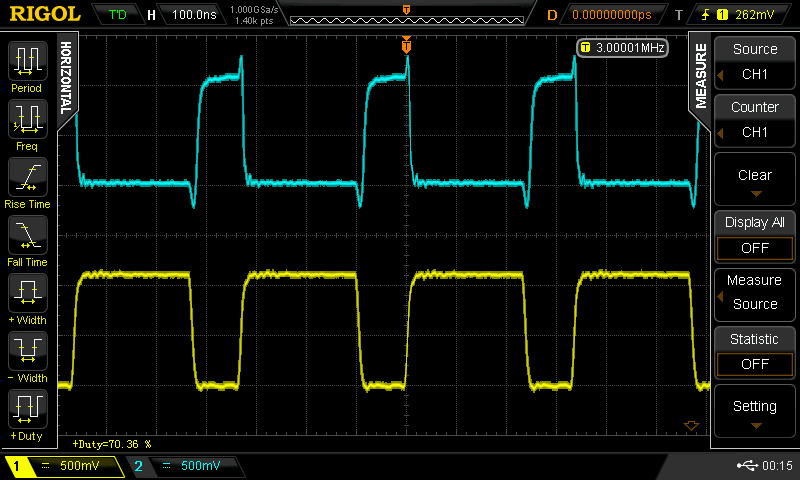 70%
70%
 80%
80%


 Bud Bennett
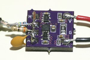
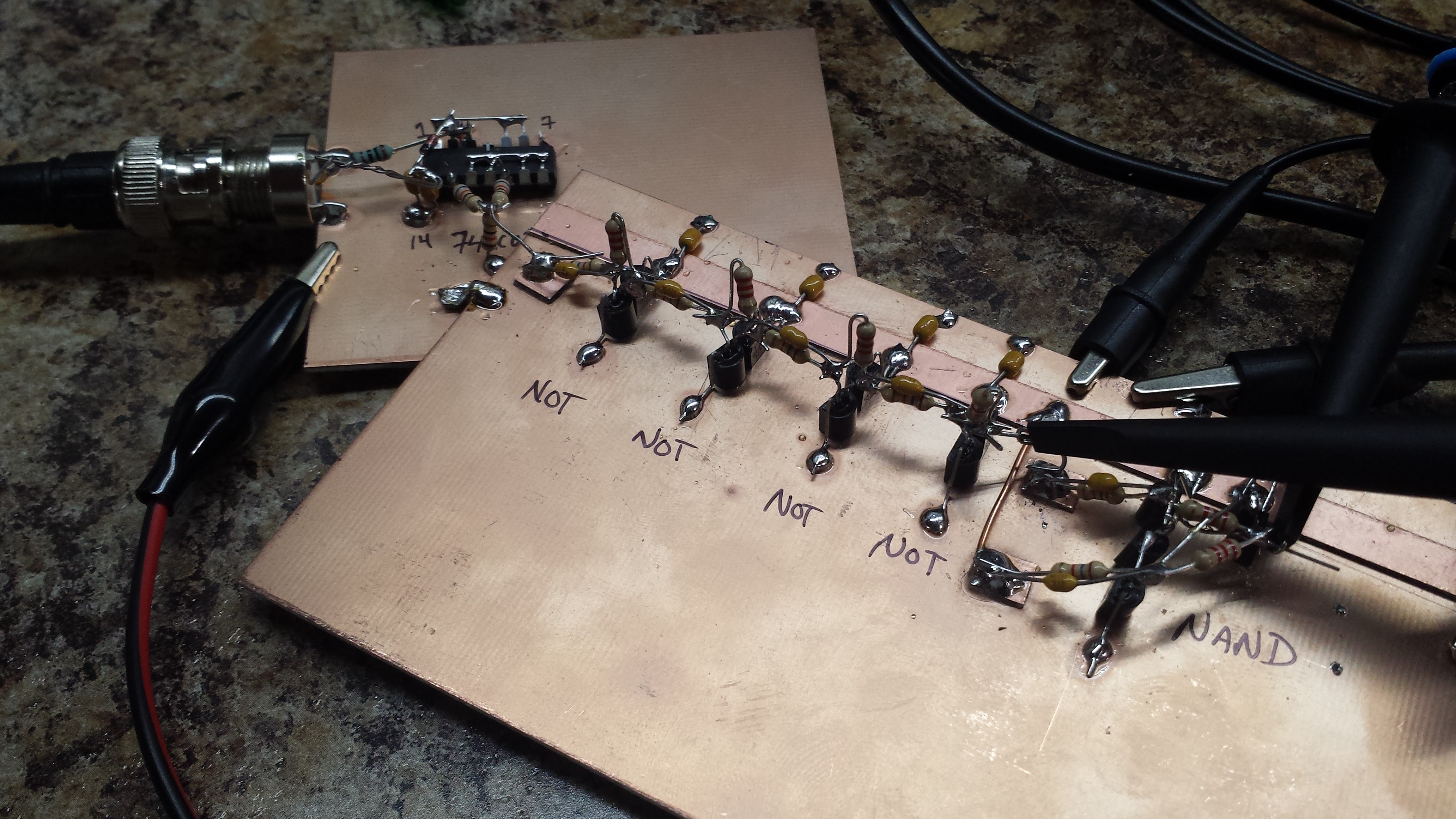
Symmetrical Transistor Logic R.H.Baker 1958 and other documents/books about transistor's logic :
http://marc.retronik.fr/old-logic/?dir=Transistors