UPDATE: the speeds measured here don't represent the true switching speed of these gates. See this log for more details.
I built a test jig for the simple NAND gate design. In order to drive it with "native" logic levels and impedances, I buffered the output of my signal generator (set to 1.1 V output amplitude) through a string of four inverters. This should produce close to a real CBJT drive for testing the NAND.

The gate design is as it was before: two 2N3904's in series on the low side, with two 2N3906's in parallel on the high side. I tested and simulated with a 1.1V supply.

At DC, the NAND gate works as expected. To test the high-speed performance, I drove one of the inputs while holding the other high. This turns the NAND into an inverter, and allows testing of the AC properties of the gate. Since the low-side transistors are in series, the two inputs are not identical - this caused the funny threshold seen in previous DC simulations.
The upper input behaves roughly as expected with the lower input held high. Here's the waveform at the upper input (yellow) and the output (cyan) when driven at 1 MHz:
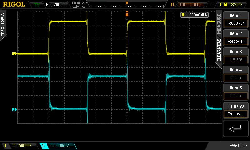
I measured the propagation delay as 9.5 ns for the H->L output transition and 4.7 ns for the L->H using cursors. The scope's auto-measurement came up with 7.48 ns and 4.5 ns for the same delays. Close enough - and not bad, really.
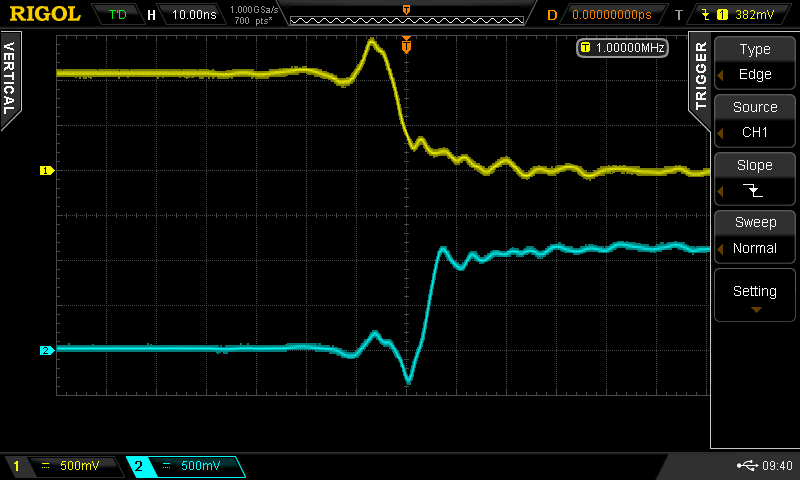
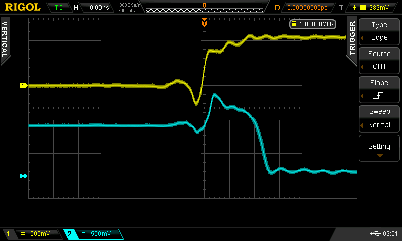
Testing the lower NAND input was much more interesting. There was a much bigger difference between the two propagation delays. Again, testing with a 1 MHz input signal, I measured 5 ns for the propagation delay when the output was going L->H - about the same as the upper input. But, the propagation delay for the other transition (H->L) was 20.7 ns, much longer than the upper input! Here's the L->H at ns delay:
vs the H-> at 20 ns:
I found this odd, partly because I hadn't seen any evidence of this in LTspice simulations. There, the delays are roughly identical:

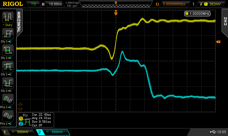
Two things come to mind: it could be bad spice models or parasitics in the layout. But playing around a bit found something even more odd - the delay depends on the input pulse frequency. At 1 MHz input, the delay was 20ns - this grew to a maximum of around 40ns with a 5 MHz input, but then the delay abruptly dropped again at 6 MHz! It was also clear that there was some instability involved - you can see in the the 6 MHz cyan trace (lower right). Here are 1, 3, 5, and 6 MHz plots. The output also peaks above the supply voltage before the transition ( you can also see this in the simulation above).
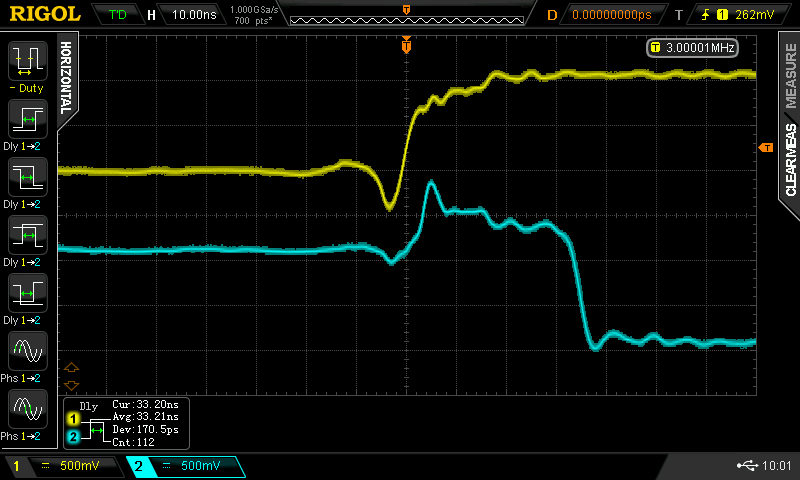
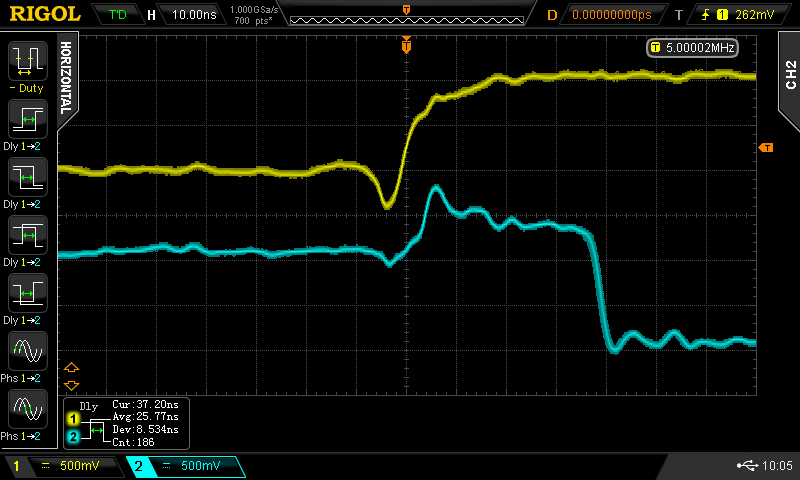
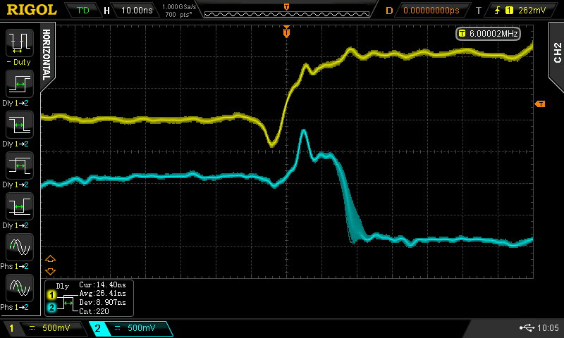
I probed around a bit, and found the problem (but not the solution) - there is some odd resonance on the node between the two 2N3904's. Here are the waveforms at that node (cyan) at the same frequencies:
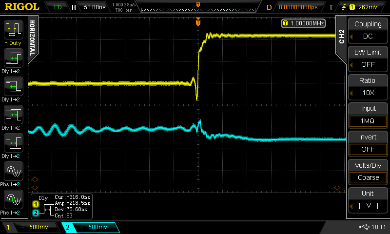
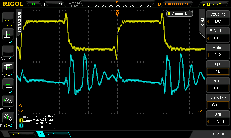

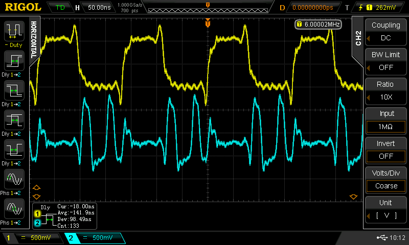
You can see that the ringing starts when the input signal goes low. For long pulse widths, the ringing has died down by the next transition. For shorter widths, the ringing can interfere with the next edge, extending the delay time by an amount that depends on what phase of the ringing the edge coincides with.
I still don't know where that resonance is coming from. It doesn't happen in the simulation. I'll have to spend some more time with the board to figure it out. I think this can be fixed. Maybe it's just poor layout on the prototype.
Even if this is an unavoidable feature of these logic circuits, this behavior will just limit the maximum usable clock frequency.
Misc. Observations
It was a bit of a mystery how the output stage switches so quickly - shorter than the transistors should be able to turn off. I looked at the simulation closely - the transistors are still slow to turn off, but the opposing one turns on quickly and dominates the output. This causes some huge shoot-through current spikes in the output stage. It may be enough to warrant a bypass capacitor per output pair. This is just something you'd need to work around if you wanted to use this logic to build something.
The common LM317 "adjustable" regulator is a fixed 1.25V regulator in disguise. Just ground the adjustment pin and use it like a 78xx 3-terminal regulator and you get 1.25 V nominal output. One datasheet I read listed between 1.2 and 1.3 guaranteed, which might be a little much.
I've been thinking about a temperature-compensated regulator based on a couple of transistors as sensors and an LT3080 adjustable regulator. This would track the transistors Vbe and keep the supply in the sweet spot with variations in ambient. Of course, all the transistors would have to be at the same temperature for this to work - or close enough, anyway.
I don't have any immediate plans for this logic; other than trying to figure out this ringing business, I think I'm going to move on to other projects. But, I might design some boards for MMBT3904's and MMTB3906's in SOT23 packages because they're so small and cheap (as are 0603 R's and C's). Maybe a quad NAND or NOR gate and an edge-triggered flip flop. It would be interesting to wire up a counter and see how fast it will go.
 Ted Yapo
Discussions
Become a Hackaday.io Member
Create an account to leave a comment. Already have an account? Log In.
So in the end, how does the corrected NAND work ?
Lately, in a different but related subject, I looked at the "cascode" (or "cascade") which is meant to reduce the Miller effect. This is another factor to consider, parasitic capacitance doesn't become too obvious with the interter gate but 2-input gates are trickier...
Are you sure? yes | no
Upper input driven:
L->H output transition propagation delay ~ 5ns
H->L output transition propagation delay ~ 10ns
Lower input driven:
L->H output transition propagation delay ~ 5ns
H->L output transition propagation delay ~ 20ns (varies 15-20)
So, on a datasheet you might write (20 ns typical propagation delay). You might be able to take advantage of some of the faster delays by some tricky design, or just assume 20ns for everything.
Are you sure? yes | no
sounds nice... you put the "late arriving signal" on the fast path...
Are you sure? yes | no
Nice work!
I wonder if the ringing has to do with C5 attempting to keep Q11's Vb constant while its Ve drops, and something to do with the switching delays...? I wonder what a resistor (or diode? maybe even a capacitor?) across VBE would do
Are you sure? yes | no
also, for some reason that node seems to me similar to that of the "floating" node between two series capacitors... seems like a great place for resonance. Maybe a voltage-divider to bias that point, and "dampen" the oscillation?
Unrelatedly, I'm sure you knew this was coming: wonder what'd happen if the top(?) transistor had its C and E reversed ;)
Are you sure? yes | no
Maybe if you reverse the C and E on one of them, you can make the whole thing with just NPNs (or PNPs)...
Are you sure? yes | no
@Ted Yapo, I had a vague inkling about that, as well... *I* wasn't able to pen-it out, but that doesn't mean anything.
Are you sure? yes | no
C5 and Q11 are the key, and I think I got it figured out now. What isn't in the picture is that I used a regular alligator lead to tie the upper input to +V. A long regular alligator lead with serious inductance and delay. If I add a few hundred nF of inductance between the upper NAND input and +V, the simulation rings like the bench test.
I haven't had a chance to try it on the board yet, but I suspect just soldering that input directly to the rail instead of using a long wire will cure the problem.
It's a little bit of a quirk that you need to worry about lead lengths and inductances for DC signals, and that the reverse isolation isn't great. The output impedance of these gates is so low, though, that maybe it doesn't matter.
Are you sure? yes | no
Always use short leads and decoupling capacitors ;)
Oh, wait, this is an *input*... hmmm...
Yeah, I can see how this system would be extremely sensitive to such things, what with the voltage-levels being so low, and your prediction about thermal effects.
Was vaguely contemplating whether replacing Q11/12 with the input-methodology of TTL (emitters tied to inputs, bases pulled up, collectors tied together as an output to make an AND) could replace that series setup, but would need an inverter inbetween... And, sounds like you've figured out the problem.
Also, I keep pondering the idea that the *input* voltages could probably exceed the rails... which might make things more immune. E.G. at the internal-logic level, run everything from 0-1V, but at the external logic-level run at -1 to 2V (or 1-2 and 0-3, respectively, for interfacing with lvcmos, no less!).
Are you sure? yes | no