 Ted Yapo
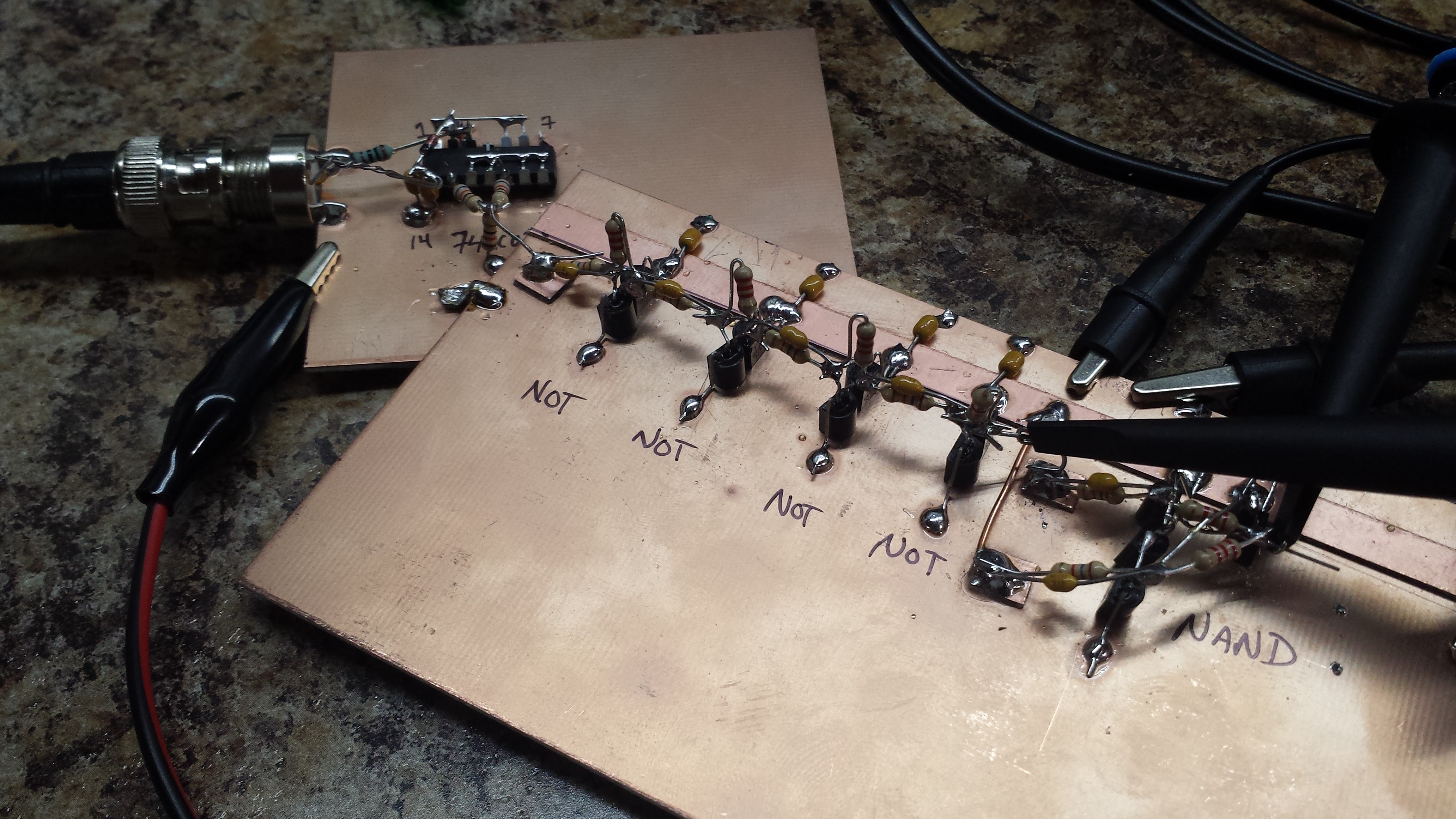
I soldered together a test using through-hole 2N390{4,6} transistors and 1.6k input / 2.2k feedback resistors. This test included four inverters driving either input of a NAND gate (also made with 2.2k feedback resistors):
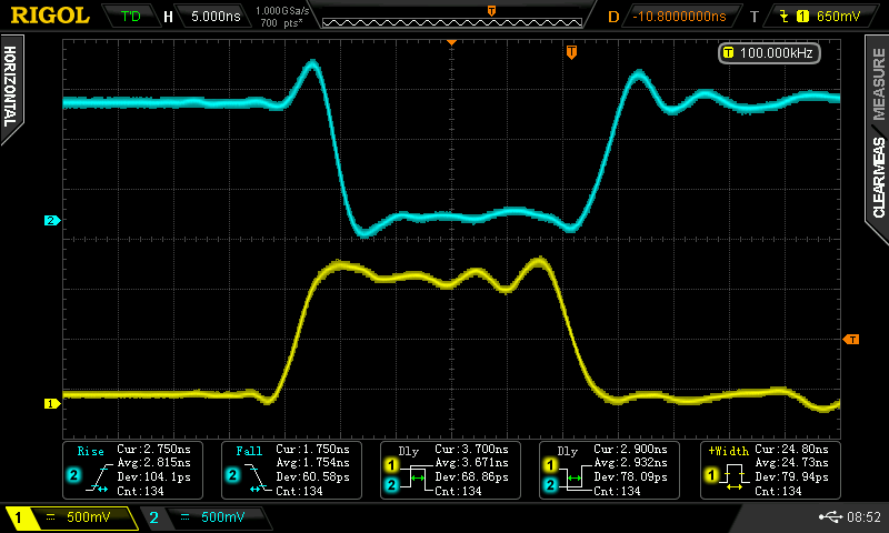
I tested this the same way I had done the SMT version: using a level/impedance/edge rate converter to drive the input with brief (~20ns), isolated (~100 kHz) pulses of either polarity. Like before, one of the output edges is delayed relative to the others, and this delay drops with input pulse length. I decided to use single, short pulses (about 24 ns after the inverter chain) to measure the NAND gate delays. This corresponds to a single pulse of a 21 MHz signal, so these results should be valid for systems clocked at this speed or below - and you can ignore the variable delay; this is a worst-case.
Upper Input Driven
With the lower input tied high, and the upper input driven, I observed the following waveforms (yellow = input, cyan = output).
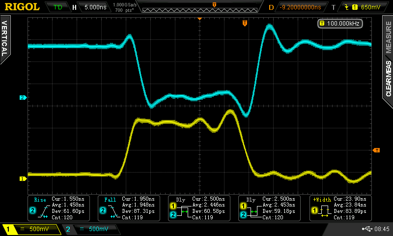
The rise and fall times vary from 1.5 ns to 3ns. These are fast edges and would require some thinking about long wires or traces in a system using these gates. With the positive input pulse, the two propagation delays are equal at about 2.5 ns. With the negative input pulse, one propagation delay is 1.5 ns (the output rising edge), and the other is 5.4 ns (the output falling edge).
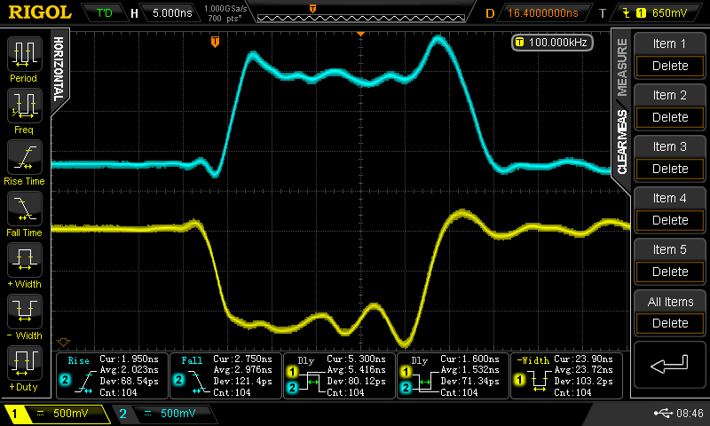
Lower Input Driven

Here, the rise and fall times are longer, ranging from 1.8 ns to 3.9 ns. With the negative-going pulse, we see delays of 2 .0 and 7.2 ns. With the positive-going pulse, the delays are 2.9 and 3.7 ns.
The 7.2 ns is the worst case of any observed - this is really the number you should think about to evaluate these gates. If you were building a small module, maybe a flip-flop or counter, you might be able to take advantage of some of the faster delays instead of simply assuming 7.2 worst-case. Generally 7.2 seems to be the number, assuming the minimum pulse widths in the system are 24 ns or more - corresponding to a system clock of 21 MHz or less.
I think the take-away from this exercise is that the feedback resistor solves the problem with isolated pulses. There are probably ways to improve things, including splitting the input resistor like was published in the 1950s. I might leave it at this, though.
Well, maybe one PCB for a counter or something, since I have the SMT transistors, and the R's and C's are dirt cheap.
Discussions
Become a Hackaday.io Member
Create an account to leave a comment. Already have an account? Log In.
Can you explain the difference of propagation delays ?
Are you sure? yes | no
No, I can't explain it. Who knows what's going on in there?
I am interested to see how a NOR gate performs.
I am also seeing some interesting things trying to simulate sequential logic with these gates (too early to post). The low gain seems to promote metastability in flip-flops and the asymmetrical delays cause some interesting hazards. It remains to be seen if a robust edge-triggered flip flop can be constructed - I haven't seen one yet. But now instead of just throwing things together, I'm trying to analyze the races. There may be hope yet.
I'll either succeed and post it, or fail and post it. Right now, I'm in a metastable state :-0
Are you sure? yes | no
That sounds curious...
Are you sure? yes | no