 Nevyn
NevynThe infrared signals from a remote control are normally carried on a modulated signal of around 38 - 40 KHz. The aim of this stage of the project is to add modulation to the digital signals generated in the last stage of the project.
How Does Modulation Work?
Modulation works by turning on the carrier signal when we need a logic one to be output and turned off when the digital signal should be logic zero. This is best illustrated with some pictures.
Digital signal:

Carrier signal (38 KHz):

Combined output:
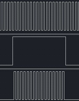 The lower trace shows how the carrier signal is only output when a digital one is to be generated. At all other times the output remains at logic zero.
The modulation is required to help devices detecting infrared signals from remote controls differentiate the remote control signal from the ambient infrared radiation in the environment from sources such as sun light.
Hardware Changes
The modulation can be generated using a PWM signal with a 50% duty cycle. This is something which is easy to generate on the STM8S. The signal output could then the turned on and off by using the timer interrupt discussed in the last post.
A simple AND gate can be used to combine the digital output signal with a PWM signal:
 A single AND gate is available in surface mount form but a standard 74HCT08 quad AND gate can be used for the prototype.
Software Changes
The software used in the last post can be reused with minor modifications. The first task is to generate a 38.4 KHz PWM signal. This can be achieved using one of the other timers on the STM8S103, namely timer 1, channel 4.
Using the default HSI clock of 2MHz the peak to peak duration of the PWM signal is 26uS. This is equivalent to 52 clock pulses on the 2MHz system clock. This results in the following setup code for Timer 1:
//--------------------------------------------------------------------------------
//
//  Set up Timer 1, channel 4 to output a single pulse lasting 240 uS.
//
void SetupTimer1()
{
    TIM1_ARRH = 0x00;       //  Reload counter = 51
    TIM1_ARRL = 0x33;
    TIM1_PSCRH = 0;         //  Prescalar = 0 (i.e. 1)
    TIM1_PSCRL = 0;
    //
    //  Now configure Timer 1, channel 4.
    //
    TIM1_CCMR4_OC4M = 7;    //  Set up to use PWM mode 2.
    TIM1_CCER2_CC4E = 1;    //  Output is enabled.
    TIM1_CCER2_CC4P = 0;    //  Active is defined as high.
    TIM1_CCR4H = 0x00;      //  26 = 50% duty cycle (based on TIM1_ARR).
    TIM1_CCR4L = 0x1a;
    TIM1_BKR_MOE = 1;       //  Enable the main output.
}
For completeness (and to save power) the PWM pulse should be turned off when it is not required. This requires a modification to the interrupt handler for Timer 2:
//--------------------------------------------------------------------------------
//
//  Timer 2 Overflow handler.
//
#pragma vector = TIM2_OVR_UIF_vector
__interrupt void TIM2_UPD_OVF_IRQHandler(void)
{
    _currentPulse++;
    if (_currentPulse == _numberOfPulses)
    {
        //
        //  We have processed the pulse data so stop now.
        //
        PD_ODR_ODR3 = 0;
        TIM2_CR1_CEN = 0;
        TIM1_CR1_CEN = 0;           //  Stop Timer 1.
    }
    else
    {
        TIM2_ARRH = _counterHighBytes[_currentPulse];
        TIM2_ARRL = _counterLowBytes[_currentPulse];
        PD_ODR_ODR3 = _outputValue[_currentPulse];
        TIM2_CR1_URS = 1;
        TIM2_EGR_UG = 1;
    }
    TIM2_SR1_UIF = 0;               //  Reset the interrupt otherwise it will fire again straight away.
}
One last change is required and that is to the main program loop, we need to turn the PWM signal on:
//--------------------------------------------------------------------------------
//
//  Main program loop.
//
void main()
{
    unsigned int pulseLength[] = { 2000U, 27830U, 400U, 1580U, 400U, 3580U, 400U };
    unsigned char onOrOff[] =    {   1,      0,     1,     0,    1,     0,    1 };
    PrepareCounterData(pulseLength, onOrOff, 7);
    __disable_interrupt();
    SetupTimer2();
    SetupTimer1();
    SetupOutputPorts();
    __enable_interrupt();
    PD_ODR_ODR3 = _outputValue[0];
    //
    //  Now we have everything ready we need to force the Timer 2 counters to
    //  reload and enable Timer 2.
    //
    TIM2_CR1_URS = 1;
    TIM2_EGR_UG = 1;
    TIM2_CR1_CEN = 1;
    TIM1_CR1_CEN = 1;       // Start Timer 1
    while (1)
    {
        __wait_for_interrupt();
    }
}
Conclusion
Connecting the logic analyser to the circuit gives the following traces:
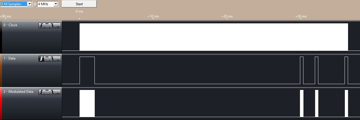 The top signal shows the carrier signal, the middle trace is the digital signal being generated and the lower trace shows the output from the AND gate and hence the LED.
The carrier signal looks like a solid block, zooming in on two of these blocks to the right of the trace shows the following output:
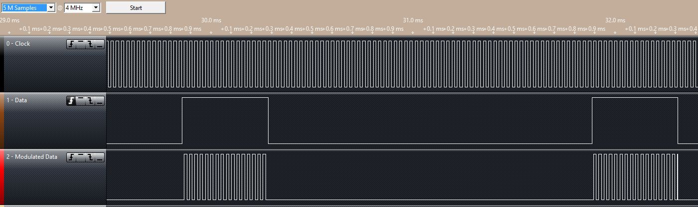 This shows the at the 38.4 KHz PWM pulse is being output as required.
The next stage of the project requires the project move from breadboard and onto something more permanent.
Discussions
Become a Hackaday.io Member
Create an account to leave a comment. Already have an account? Log In.