 Ted Yapo
UPDATE 20170207: I forgot resistors! Fixed in the addendum below.
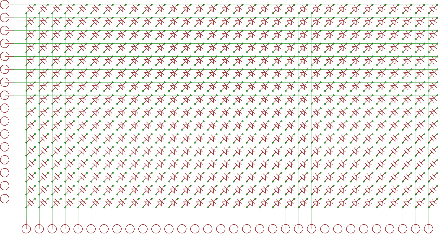
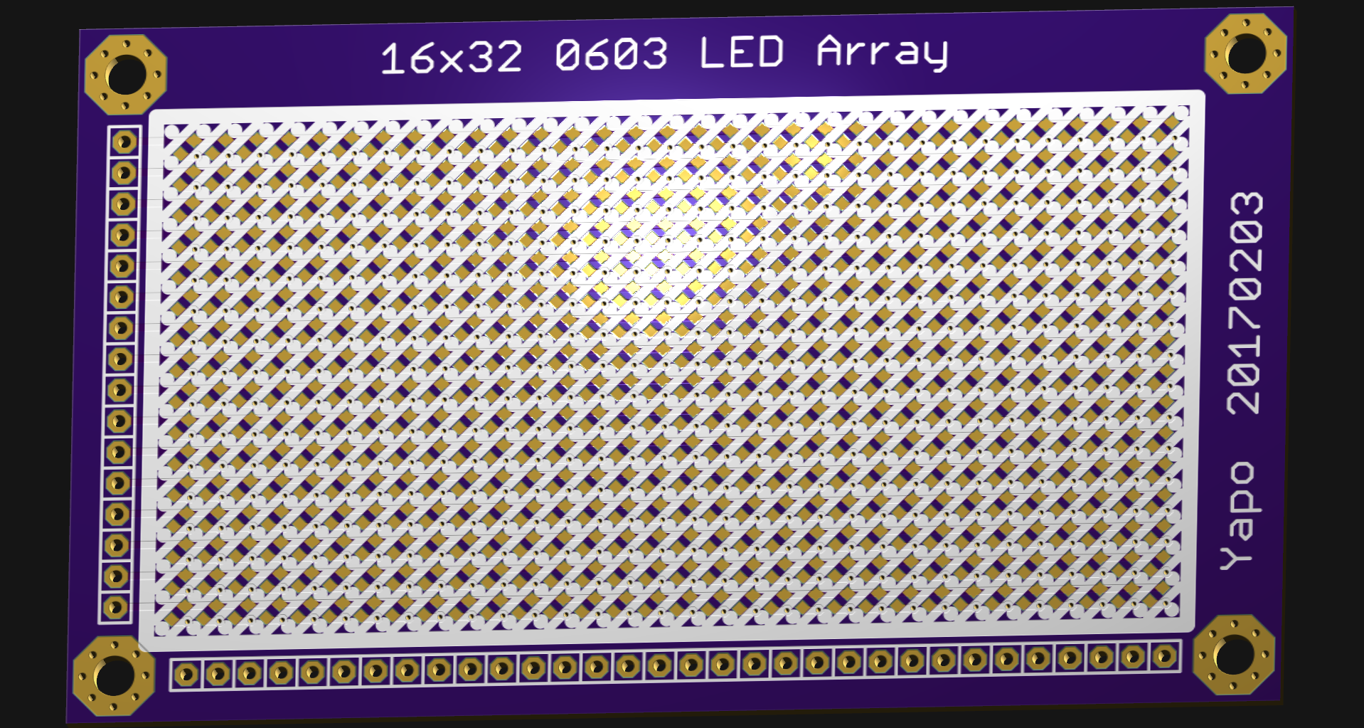
I painstakingly drew the schematic for 512 LEDs in this display, then endured the drudgery of laying out the board. The whole process took about 45 seconds. Yes, I wrote a few Eagle User Language Programs (ULPs) (elapsed time after the scripts were written and debugged). The previous time I wrote one was last century to lay out a circular LED clock face. I figured it was about time I regained those skills. The code is here on GitHub. You can edit the scripts to produce any size array. The "led_matrix_schematic.ulp" code generates the schematic. Here's the 16x32:
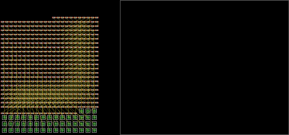
The default board (auto-generated by Eagle) looks like this:
A second script ("led_matrix_layout.ulp") re-arranges all the components and adds traces, vias, and silkscreen programatically:
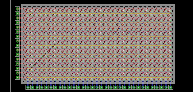
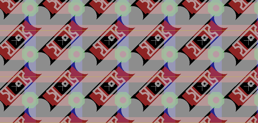
The silkscreen matrix is there to act as a reflector. I have been experimenting with 3D printed segmented bezels and diffusers which make the 0.1"-spaced tiny-die LEDs look like a closely-packed array of pixels. I'm still experimenting with a number of different diffusers from a Roscolux theatrical lighting gel swatchbook - I'll post images in an upcoming log. The short story is that you can make these matrix displays look like a nice pixel array, but at the cost of some efficiency. I think that using the silkscreen to reflect light off the board will improve the brightness - and it's free, so why not. There's a flag at the top of the script to turn off all the reflector silkscreen segments if you don't care for them.
The scripts rely on an Eagle library ("led_matrix.lbr" - also in the GitHub repo) I created that contains only three parts: the 0603 LED, a 1-pin 0.025" header, and a #4-40 or (M3) mounting hole. You need to add this library to your project before running either script. The mounting holes aren't automatically placed, so you'll have to do those manually, as well as sizing the board and adding any desired text.
If you run this script, you may be concerned to find "unrouted" airwires on the board (shown below).
The problem is that I can't figure out how to programatically "route" nets to Eagle's satisfaction. Instead, I draw traces on the appropriate layers. In some cases Eagle recognizes the electrical connection, and in other's it doesn't. Part of the problem is that the LED package is metric, while the board is in inches. Add to that the irrationality of rotating the LEDs 45 degrees, and the imprecision of floating point representation, and it's not surprising that Eagle loses track of things. If this concerns you, you can verify for yourself that all the tracks are in order.
If you make one of these boards, you will also want to adjust your design rules to "tent" the vias - cover them with soldermask. This should enable them to carry the silkscreen, too.
Here's a rendering of the final test board. I am going to wait a day before sending this out just in case I think of anything. I usually do.
ADDENDUM
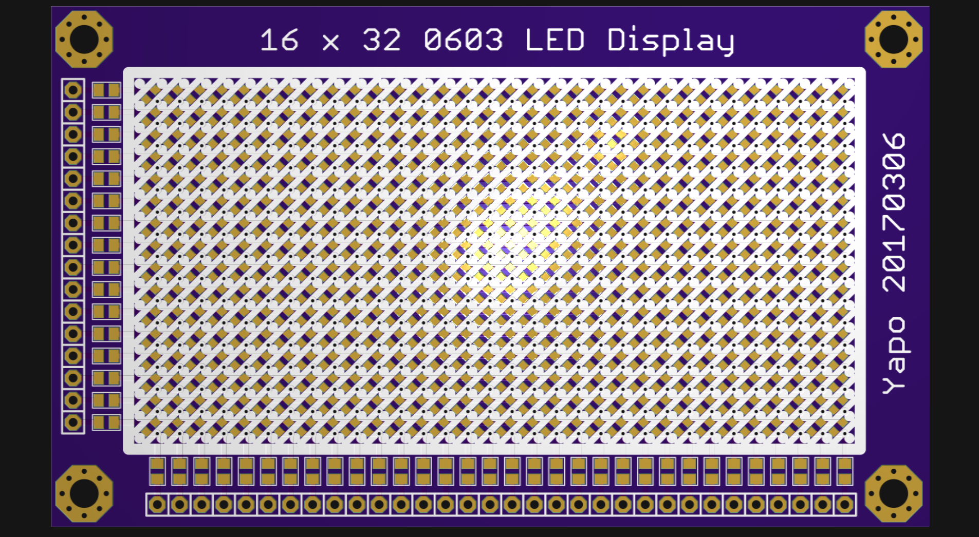
I forgot to include resistors on the board - I'm glad I waited to send this one out! I just updated the GitHub repo with code that adds 0805 resistors in each row and column. At low speeds, you really only need one or the other, but I am planning to use both on higher-speed versions to damp ringing on the row and column lines. It's not really possible to maintain a controlled impedance on the lines, and I'm concerned that any ringing may end up visible as ghosting on the LEDs. By splitting the required dropping resistance across the row and column lines, I may be able to hide these effects.
Now I'll send it. Sent!
In the two weeks before the boards return, I can look at fast sweep generation with 74AC164's and some simple ADC tests with an AD9200 ADC (because I happen to have about a hundred of them lying around).
Discussions
Become a Hackaday.io Member
Create an account to leave a comment. Already have an account? Log In.
I added dialogs for parameters and a 2.0mm pitch pattern which manages to pack 16x48 LEDs into 100x38 mm (minus the resistors). A partial design rules file gets merged to tighten the stop mask expansion and cover up closely placed vias.
https://github.com/MisterHW/led-matrix-generator
Are you sure? yes | no
Oh my! Can't wait for the 32x56 version ;-)
Are you sure? yes | no
I tried ... 32x56 doesn't fit in the 80x100 mm Eagle light edition :-(
I may have to subscribe to the new Eagle plan to try 160x100 mm for a few months. Even then, it might be a tight squeeze.
I am able to place the LEDs on an 80-mil grid instead of the current 100, but populating the board might be more difficult, and 100-mil centers are nice for the connectors.
Are you sure? yes | no
Just throwing random idea - can't you divide the layout into two (or more) separate boards, intended to be next to each other? I can imagine the design rules on the edges could be violated, depending on manufacturers limits.
Are you sure? yes | no
@jaromir.sukuba Sure, an 8x8 tile might be ideal. But then, I'd want them lined up perfectly, so I'd make a main board to plug them all into to keep them lined up. At that point, they might as well be on the same board. Someone with less obsessive tendencies might have better luck with such a strategy :-)
I guess the only snag might be where to put the header pins - if you have tiled boards, you can't have the headers on one side. I guess splitting the boards in half would work - which may be what you were suggesting - OK I get it now - yeah, maybe that's a way to make 32x56 with Eagle light edition. Good idea.
I'll have to consider this :-)
Are you sure? yes | no
Or you can make solder pads (for the rows) on the edges that you use solder bridge to tile them up like LED strips. Add in a via/hole for each of the pads so that they don't get ripped. They can also be tiled together with solder wire for more strength.
Are you sure? yes | no
@jaromir.sukuba , @K.C. Lee good suggestions, both. I think the real problem here is that I'm up against the limitations of a free version of commercial software (Eagle). One solution would be to move to KiCAD, but I have little experience with it, and don't even know if it has a programming interface.
What would probably be easier for me at this point would be to just write out gerbers (and a drill file) directly from python code. They're just text files, and not particularly complicated ones. With this design, there's really no need for a schematic at all - once you've seen one diode array, you've seen them all. Gerber previewers abound (even I wrote one - it generated the 3D preview above), and the fab doesn't know where the files came from. It's probably a day or two worth of work to put together, but might be worth it in the end.
Are you sure? yes | no
I remember one hack somebody used long time ago to workaround limitations of free version of Eagle - designed all parts half of the size, and printed the PCB magnified 2x. Perhaps one can do "magnification" in gerber data too.
Switching to KiCad is possible option too, but from my experience, it's not 100% fit for everyone. Some people claim it is awesome compared to Eagle, some others think it's clunky and painful to use. Personally, I'm trying to switch to KiCad from 2011 or so, every year.
Are you sure? yes | no
@jaromir.sukuba that is a really ingenious solution to the size limitation. The library files are all stored in XML files, so I could imagine a program tearing through and making half or quarter sized versions of all the libraries automatically. Another program would expand the scale of the gerbers by an equal factor after the design. You might need to fool around with the number of decimal places in the gerber files to maintain the required precision through the modified toolchain, but I bet the whole thing is possible.
Maybe make it a factor of 10 to make everything easier. Now your limits are 800 x 1000 mm in the free version. I've used Eagle for two decades, and I really appreciate them making a free (and previously inexpensive light) version, so I shouldn't try to build such a system. On the other hand: hack.
Are you sure? yes | no
The x2 "hack" is because printer output allows only 2x maginfication. When dealing with gerber data, you can multiply everything by 10000/254, switch eagle to mils and use is as milimeters, while enjoying 3x4m of working area. Or multiply everything by 25.4 and use milimeters as inches, having 100x80 inches of working area.
Are you sure? yes | no
Impressive!
Are you sure? yes | no
Thanks. We'll see how my hands feel after mounting all those LEDs :-)
Are you sure? yes | no