 esben rossel
The sensor in the Raman spectrometer is the linear CCD module. However, because the CCD drowns in dark current when the integration time is longer than 1s, the TCD1304DG is mounted on a cold tip that's thermo-electrically cooled using a standard TEC1-03506 running at 4.2V (but the photograph shows the CCD with a TEC1-12706).
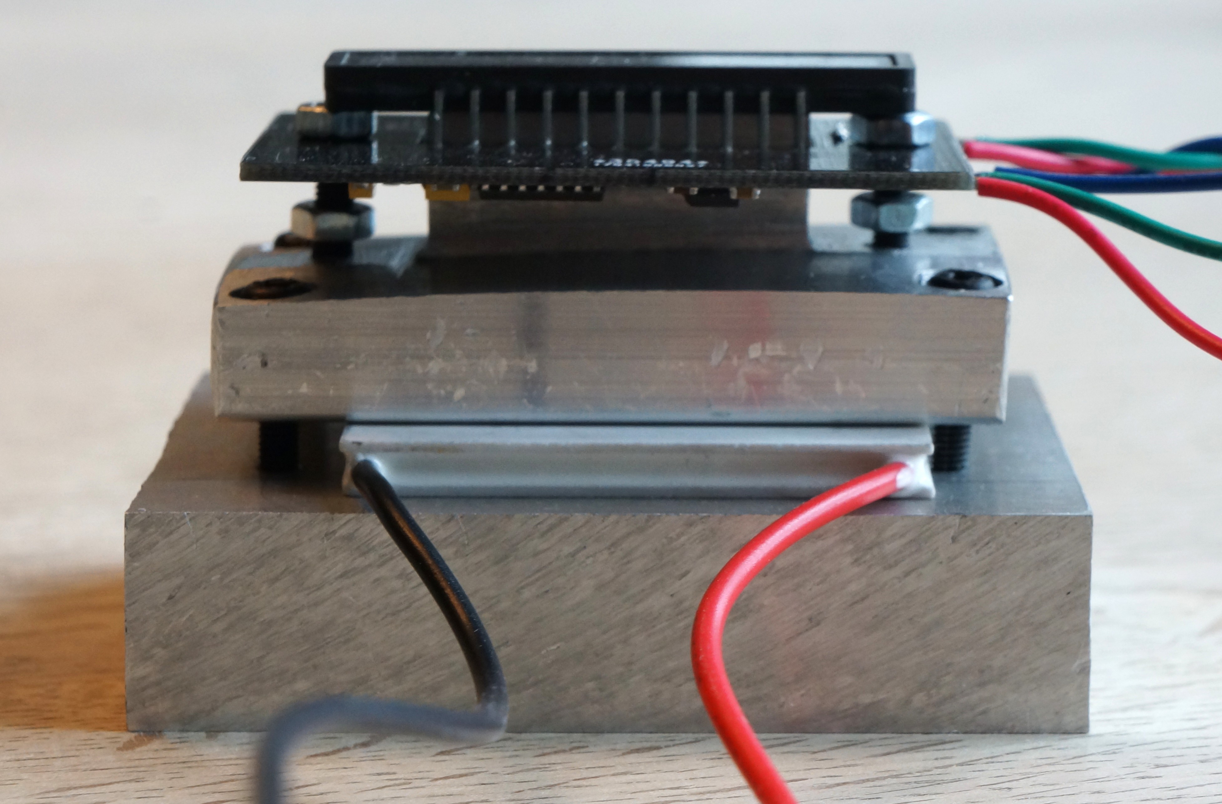
Here it is with the right peltier element. The temperature drop was ~25°C, which gives a reduction in dark current of almost an order of a magnitude. Of course it caused a lot of condensation on the CCD, but when complete, the spectrograph will be sealed up together with bags of dessicant.
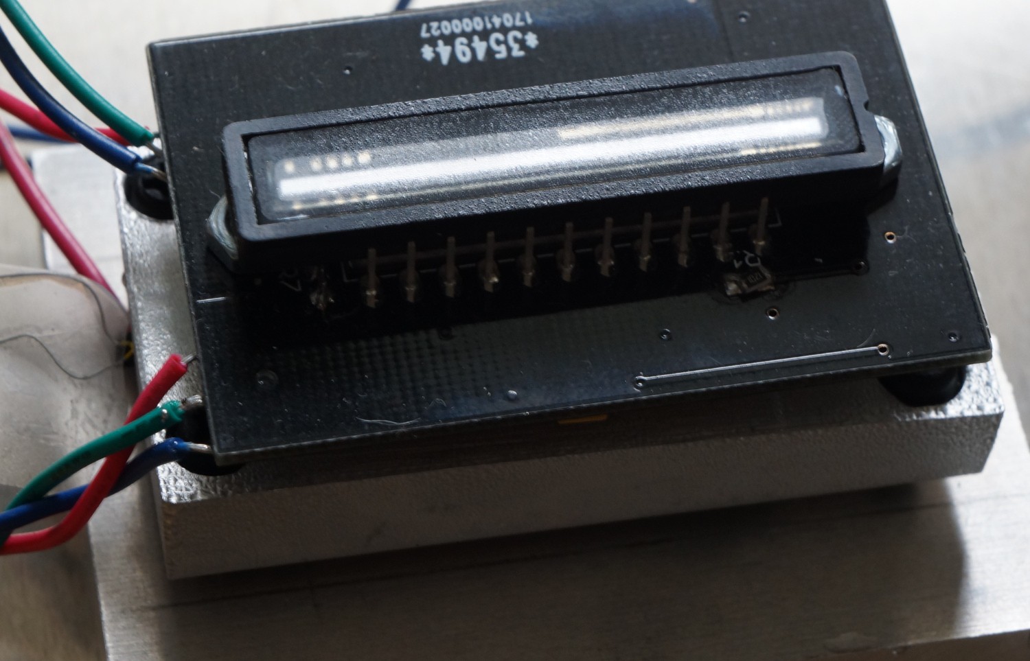
An STM32F103 "blue pill" connected to a 10kΩ thermistor mounted on the cold tip displays the temperature on an ILI9341 display.¹ The voltage drop across the TEC is also measured, just not at the time the photograph was taken. The firmware may be found in the files section of the project.

Furthermore, the CCD is placed in a more elaborate circuit than the datasheet's typical drive circuit.
The most notable new features are:
- ADC input signal conditioning
- Separate power supplies for the digital and analog sections
The
output from the CCD is upside-down and doesn't quite match the ADC of
the STM32F401RE's input range of 0-3.3V. To fix these issues the output
is fed to an AD8021 opamp² working as a differential amplifier:

The gain is:
G = - R₂ / R₁
we have an input range of 1.9V (2.5-0.6V), but want 3.2V (actually 3.3V but I don't want to risk clipping the signal), so G should be -1.68.
The level shift is:
S = R₄/(R₃+R₄)·(1+R₂/R₁)·Vref
The output voltage then becomes:
Vout = G·Vi+S = -R₂/R₁·Vin + R₄/(R₃+R₄)·(1+R₂/R₁)·Vref
There’s probably a point to the resistor values in the typical drive circuit (noise?), so R₁ is chosen to be 150Ω. The gain then dictates that R₂ should be 252Ω. Setting Vref to 5V (it is in the complete circuit) R₃ and R₄ can be found by solving:
Vout = 3.2V    when Vin = 0.6V        and
Vout = 0V      when Vin = 2.5V
One solution is (almost) R₄ = 150Ω and R₃ = 330Ω
The CCD-circuit in its entirety is shown here:

If I were to redo it, I would substitute the 78L05 and 79L05 voltage regulators (U3-4 and U2) with LDOs LT1761 and with LT1964.
[1] The LCD is driven using fagcinsk's stm-ILI9341-spi library.
[2] I can't take credit for this, I stole parts of the circuit from David Allmon.
Discussions
Become a Hackaday.io Member
Create an account to leave a comment. Already have an account? Log In.