 PointyOintment
An alternative to serial processing such as is done by a CPU is programmable logic. In programmable logic, one defines a circuit of logic gates that achieves a desired result and programs this into a programmable logic device (PLD). Programmable logic devices include, in reverse order of invention and power:
- Field-programmable gate array (FPGA)
- Complex programmable logic device (CPLD)
- Generic array logic (GAL)
- Programmable array logic (PAL)
(The PLD type names all seem very similar and non-descriptive. I doubt anyone could tell which name corresponded to which architecture without being told.)
An FPGA is a device that, instead of having a (mostly) fixed circuit that performs computations according to a program, allows you to reconfigure its logic gates to form any circuit you want. It uses a different architecture than previous PLDs, specifically, using logic based on lookup tables (LUTs) instead of the pure gate-based logic used by the earlier PLDs. The "field-programmable" in the name simply means that it is programmable after leaving the factory, as opposed to a non-programmable logic chip, which is permanently configured at the time of manufacture.
FPGAs are used in many applications, including real-time processing, glue logic, and prototyping of application-specific integrated circuits (ASICs). Originally they competed in the glue logic market with CPLDs, but they soon grew into other markets as well, adding dedicated logic circuitry such as multipliers, which enabled their use for digital signal processing (DSP). Some modern FPGAs also have integrated CPUs and RAM.
Architecture
Logic blocks
The base unit of the FPGA architecture is the logic block (aka configurable logic block, logic array block, logic element). This is a circuit that can be programmed to emulate any kind of Boolean logic gate. A diagram of a simple logic block is:
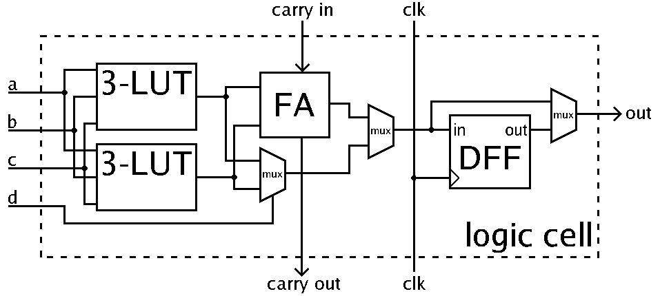 Diagram by Petter.kallstrom, public domain
The basic components of the logic block are two three-input LUT or a single four-input LUT, a full adder, and a D-type flip-flop. Between these components are multiplexers, which determine the routing of the signals through the logic block.
The left mux combines the two three-input LUTs into a four-input LUT. Some modern FPGAs have an actual four-input LUT instead.
The center mux is used to switch between normal mode and arithmetic mode. Normal mode means the output of the four-input LUT is passed to the right third of the circuit, while in arithmetic mode, the outputs of the 3-input LUTs are combined by the full adder and its result goes to the right third. (The full adder and the LUT-combining mux both always operate; the middle mux just chooses which of their outputs to use.)
The right mux is used to switch between the synchronous and asynchronous output modes. In synchronous mode, it takes the output of the D-type flip-flop, which passes on and holds its input signal upon receiving a clock pulse. In asynchronous mode, it takes the output from before the flip-flop, resulting in the output not waiting for the clock signal.
Together, all of these components can be programmed to emulate any Boolean logic gate. There may be hundreds to thousands of these logic blocks in an FPGA.
Hard blocks
Modern FPGAs also have hard blocks, which are dedicated logic circuits such as transceivers, multipliers, memories, and small CPUs. These are built in the normal way, as ASICs, instead of using logic blocks. This enables them to be much faster and more efficient, and leaves the logic blocks unoccupied for the user's circuits.
Routing
An FPGA also has switching components that connect the logic blocks to each other and to the hard blocks. The switches are individually programmable just like the logic blocks are. They are typically found between all of the logic blocks, though some modern FPGAs share switches between several logic blocks to increase speed.
The logic blocks and the switches form what is called the FPGA's fabric, in which the logic blocks are themselves programmable and are interconnected in a programmable way by the switches. This enables the user to create any logic circuit they desire within the FPGA (as long as the circuit can physically fit within the number of logic blocks the FPGA has and can be laid out such that the signals are routable).
FPGA programming
Whereas with a CPU one gives it instructions one-by-one and the chip executes them one-by-one, with an FPGA one gives it a circuit and the whole circuit is loaded into the programmable logic fabric and run all at once, continuously.
There are two main ways to design these circuits: hardware description languages and circuit schematics. The two most popular HDLs are Verilog and VHDL, though there are several others. Schematics have fallen out of favor because they are less efficient than HDLs for the large designs that commercial FPGA users create these days. However, some people find schematics easier to learn than HDLs. (The Papilio Arduino-like FPGA development board ecosystem emphasizes schematic-based design for this reason.)
FPGAs can also be designed for by other methods, such as LabVIEW, MATLAB/Simulink, and OpenCL.
Pre-existing circuits, called IP cores, are available to simplify designing FPGA circuits by providing common functionality that's already developed and tested. Some of these are free and open-source, while some are commercial.
However one designs a circuit, it must then be prepared to be flashed to the FPGA. The first step is to convert the high-level logic design written by the user into a circuit of logic gates, a process called logic synthesis. The logic gate circuit is then laid out so that it will fit into the FPGA and all of the signals can get where they need to go without colliding, called place and route. At each stage, the circuit is simulated to ensure the produced circuits will perform correctly and the signals get to their destinations quickly enough. Once this is done, the circuit is converted to a bytestream which is sent to the FPGA's memory. (This memory may be internal or external, depending on the particular FPGA design.)
Everything in the above paragraph is done by proprietary software provided by the FPGA manufacturer. There have been some efforts to create free and open-source toolchains for programming FPGAs, though so far only one has been developed enough to be usable.
Discussions
Become a Hackaday.io Member
Create an account to leave a comment. Already have an account? Log In.