The last log entry showed a CPU connected to an Arduino, where the Arduino would act as both RAM and I/O, all running via a memory-mapped I/O interface. The address bus was completely connected to the Arduino's inputs. The software running on the microcontroller would then decode the address bus to figure out the intent of the load/store operation. This is great because it allows us to do anything we want from an I/O perspective but directing all traditional memory load/store operations through that route is slow - each bus cycle would take hundreds of 68k cycles.
So let's add a real RAM chip to our system. Parallel static RAMs - the type used here - typically have a simple pin interface. Parallel ROMs are similar too.
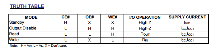
- read/write - do we want to read from the RAM or write to it? If write it consumes the data on the data bus; if read then it pushes data onto the data bus.
- chip select - this enables the chip. If enabled then the data bus works as described above. If the chip select is disabled the data bus typically goes into a high impedance state and allows the device to be effectively ignored in the circuit.
- address bus - the linear word address to be read or written
- data bus - pushed by the CPU if a write, pushed by the RAM if a read, high-Z if the chip is disabled
- some sort of 'ok, go' pin - for a read this says "the address set is valid, please now read out that address" or for a write "the address set is valid and the data to write has been loaded onto the data bus - now do the write".
- there is typically no acknowledgement pin to say the action has been performed
RAMs are organised into words and the address bus selects which word is read out on the data bus. The data bus has the same width as the word size. As the 68008 has an 8-bit data bus I'm going to use a RAM with an 8-bit word size. The address bus has the same width as the number of words (in binary bits).
Picking a RAM
I'm going to use an Alliance AS6C4008-55PCN. This is a 5v DIP static RAM with a word size of 8 bits and has 512k words...ie this is a 512 kilobyte RAM. Remember that the 68008 has a 1 megabyte address space - it can't trivially address larger than 1 MB without resorting to funny tricks, so this means the RAM can take up to half of my address space.
This part has a ~55 ns max read cycle. This means that once the "ok, go" pin is asserted the operation will complete in ~55 ns. We're getting ahead of ourselves here a bit but this is fast enough for this CPU at the clock speeds we want to run at (at 4 MHz each clock cycle is 250 ns long and it takes four clock cycles to do a whole bus cycle...of which the RAM has roughly two clock cycles to do its thing. So ~9x more time than we require)
Connecting the RAM
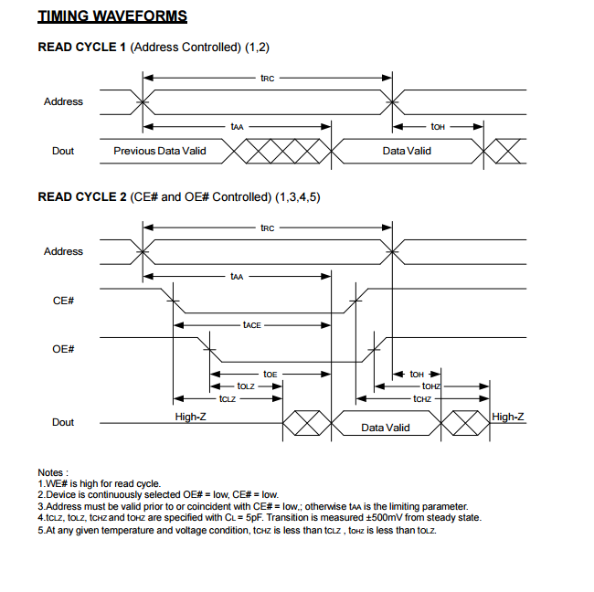
This RAM has three interesting control signals: chip enable (/CE), output enable (/OE) and write enable (/WE). Here's the truth table and the waveform timing diagram.
If we only want to connect the RAM directly to the CPU then this is easy.
- The RAM's /WE is connected straight to the CPU's R/W signal. R/W is high for read, low for write which maps directly to the Dout and Din behaviour shown above.
- The /OE is tied low
- /CE is connected to the CPU's /AS. When /AS is low, the address on the address bus is valid. 55ns after /CE is changed the RAM will hold the data on the data bus (and will continue to do so as long as nothing changes). The CPU will latch the data from the data bus at the end of its bus cycle and then negate /AS once it has done this. The write waveform works in a similar fashion.
- we connect the 8-bit RAM data bus directly to the CPU's 8-bit data bus.
- we connect the 19-bit RAM address bus directly to the CPU's A0-A18 address bus. This leaves A19 floating.
- notice the waveform is asynchronous - there is no clock driving any of this stuff.
As we have no other device in the system - it's just the RAM and CPU, and no Arduino - and the RAM has an access time faster than what the CPU requires, we can just tie /DTACK to ground, constantly asserting the signal. This will mean that when that the CPU will never insert any wait states for a memory operation. As mentioned earlier, The CPU gives a ~2 clock cycle window for the memory to do its thing and at 4 MHz that's about 500 ns. Therefore if the RAM were ~9x slower we would need to introduce wait states. So keeping /DTACK asserted is good enough for now.
The memory map
The CPU has a 1 MB address space and memory operations present the address associated with a bus transfer onto the 20 pins of the address bus. As we have not wired the top pin to anything it is ignored by the system - reading/writing to address '1' will present the same address to the RAM as address '524289' (that's 10000000000000000001 in binary). Reading from any address 0<= addr <524288 will return the same value as 524288<= addr < 1048576.
We have mapped the 512 KB RAM block into two locations in our 1 MB address space - the low 512 KB and then the high 512 KB. To be explicit,
- 0x0 - 0x7ffff
- 0x80000 - 0xfffff
What next?
So our CPU has RAM, and RAM as fast as it can run. But when we power on the system the contents of that RAM is undefined. We have no program to run and there's also no I/O (so why even bother run the program?). When the CPU was connected to the Arduino we had all of those thing (but slow RAM). Next time we need to connect all three together somehow.
Discussions
Become a Hackaday.io Member
Create an account to leave a comment. Already have an account? Log In.