0%
0%
Lifetime fails project
Every person makes mistakes, wise person learns from them.
 kevarek
Become a Hackaday.io member
Already have an account? Log in.
Just one more thing
To make the experience fit your profile, pick a username and tell us what interests you.
Pick an awesome username
hackaday.io/
Your profile's URL: hackaday.io/username. Max 25 alphanumeric characters.
Pick a few interests
Projects that share your interests
People that share your interests
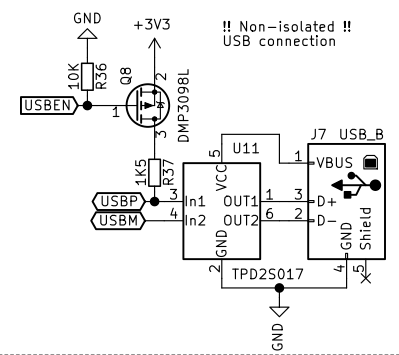 Well few days ago, while reusing one of my very old and obsolete PCB without external switchable pull-up, I had to write new firmware and each debug session start I had to re-insert the connector, which was mind numbing and after some time I started to look for software workaround. Im not sure whether this is USB compliant hack, but it certainly works.
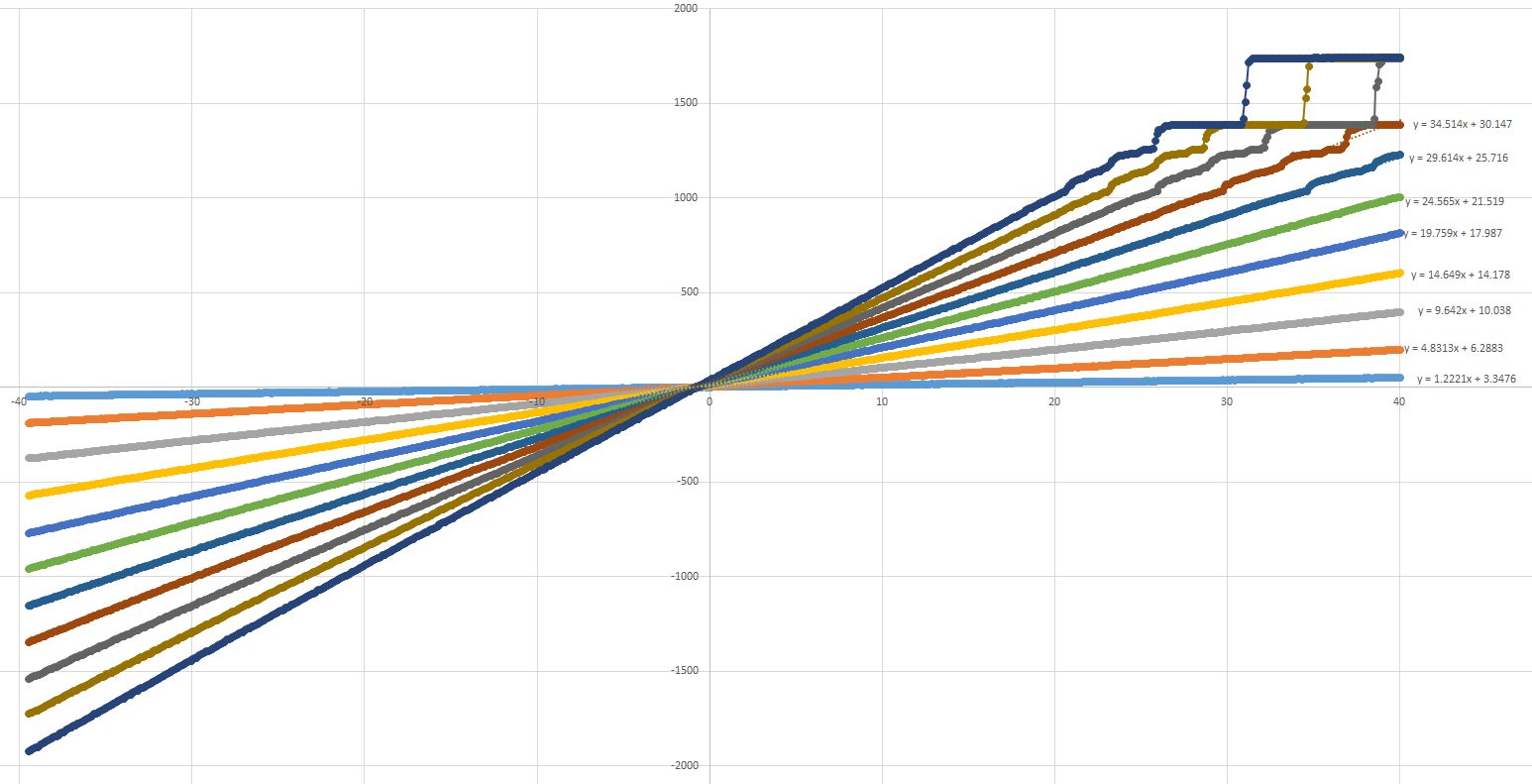
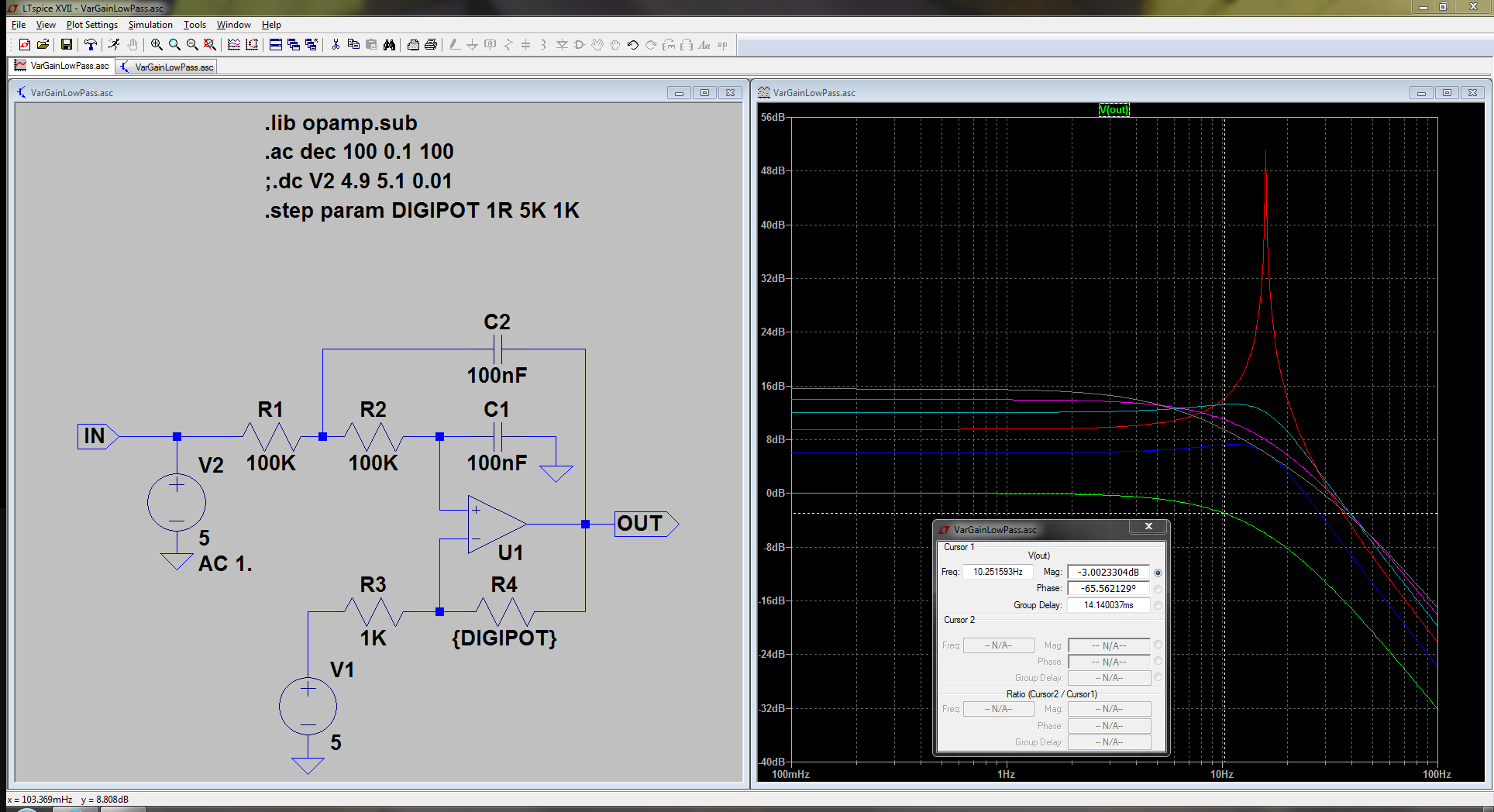 Frequency simulation from 0.1Hz to 100Hz for same gains reveals the reason. The filter with gain 2x tends to amplify extremely frequency about 10.5Hz, phase shift goes above 180° (not present on plot above) and positive feedback via C2 causes the oscillations.
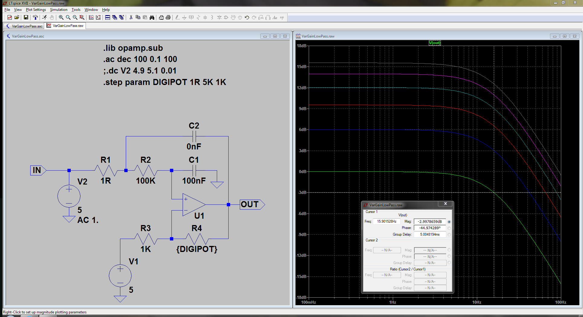


 Amos
Amos
 Dhruv Gramopadhye
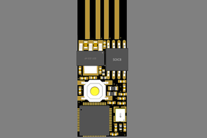
 TEC.IST
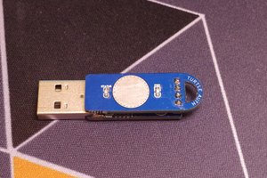
 Samuel
Hey kevarek, this is very cool, really and what timing you have. I have been doing research on using cmos web cam (the JDEPC-05) for use as a spectrometer detector's image sensor, well, it did work until I changed my spectrometer design (which was planned,) to a more sophisticated design for Raman spectroscopy, (czerny-turner configuration.)
I overlooked one critical factor throughout the entire time, that the cmos sensor was able to work because it only had to translate the incident light image as it struck the DVD grating only 2mm away from the lens, with my new design ( a two mirror design,) the image strikes the 1st mirror, then strikes the diffraction grating, which in turn strikes the 2nd mirror, which focuses the image towards the detector.
Out of the year that I have been doing this, one would have thought that I would have realized that once the image leaves the 1st mirror and strikes the diffraction grating that, the image is dispersed into it's constituent and respective wavelengths before every string the 2nd mirror...what did that mean? big fat DUH!
A spectral image ( from blue to red,) spread out about 50mm wide! Lesson learned, (after 600 pages of research notes,) always pay attention to the small details :)