 Eric Hertz
UPDATE: Whoa Whoa Whoa..... (at the bottom).
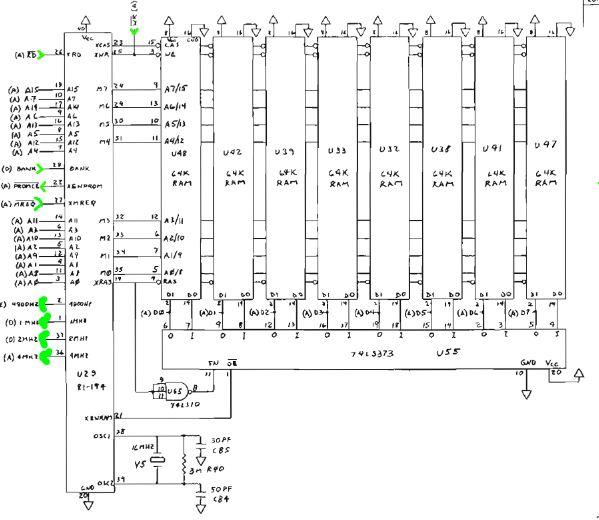
So, the question, earlier, came up regarding how the DRAM gets refreshed, if the /REFRESH pin is N/C (which it appears to be, according to the schematic).
and dammit if I didn't have a long write-up on the matter, and lost everything after this point. So, I guess I'll get to the point.
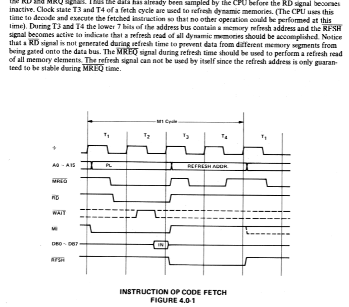
There's really no *need* for the /RFSH signal. At least with typical DRAMs. Basically, a row in the DRAM is refreshed whenever a row is accessed. And for a typical Read/Write operation, the row is accessed first, then the column, then the Read/Write signal is sent. So, the row gets refreshed with every read/write access.
So, why not treat *every* address placed on the address-bus, accompanied by /MREQ, as a Row AND Col access, as though for a read/write? And... now I'm pretty sure that's what happens.
Simple.
And I'm betting the custom chip doesn't contain any specialized logic regarding refresh.
----------
There's still the issues of BANK and /PROMCS, and how those are related to the DRAM... My guess, again, is that *every* address-access on the Z80's address-bus, accompanied by /MREQ, accesses a memory-location in the DRAM (even, for instance, when the ROM is being read).
BANK is controlled by a bit on the "system port" register... That, as we understand, chooses whether to do memory-accesses from the ROM or the RAM. So, e.g. during boot, BANK directs it to the ROM, then after boot, its directed to the RAM where the OS is stored, etc. (There's some debate as to whether the "BIOS" in the ROM is accessible to applications once the bank has been switched to RAM... E.G. if there could be, say, routines in the BIOS for displaying characters on the screen, could that be called from a user-application, switching into the ROM for execution, then back into the RAM for the next portion of the user-application? I'm sure there are ways, but they may not be pretty... e.g. storing *pieces* of the same code in both ROM and RAM, at the same locations... I'm sure I can find out with further analysis of Ziggurat's ROM disassembly).
So, obviously, when BANK is set to ROM, /PROMCS gets activated with /MREQ, but /XENRAM does not. But, then, when the ROM is executing (during boot), the RAM still needs to be refreshed... so its still feeding *every* address-access to the row/col system... Which is fine for /RD, since /XENRAM is disabled and therefore the data in the DRAM is not written to the data-bus...
But what about Write...? /WR is not gated through the custom chip, it goes *straight* to the DRAM!
Ah hah!
Write... Never Happens to the Read ONLY Memory.
OK-then...
Now this leads me to the question of how the ROM can access RAM, for storing variables, etc.
In what I've seen of Ziggurat29's disassembly, it seems the stack-pointer is set-up in a high-address, e.g. 0xff00... and it seems most other variables are stored up there, as well...
So, then, BANK only switches between ROM and RAM in the *lower* addresses, and always accesses RAM in the higher ones... simple enough.
And, again, by treating the RAM as though it's being accessed even when the ROM is, but gating the RAM's /RD signal (/XENRAM), it still gets refreshed.
This custom chip is starting to seem quite simple, really... a few gates.
(As Ziggurat29 pointed out a while-back, the 2x motherboard uses this custom chip, but the earlier motherboards are similar in design but use discrete logic instead... I've been meaning to look at those, but haven't yet. All these ramblings are from the perspective of treating it like a black-box... I guess it's kinda like doing math homework where the answers are in the back of the book... should I go look?)
-----------
Whoa Whoa Whoa!!!
that /WR signal is *directly* connected to the DRAM chips! And they don't have Chip-Selects! That's fine for ROM... but...
What the heck happens during an I/O write!?
... "/CAS is used as a chip select activating the column decoder and the input and output buffers."
So, maybe I'm mistaken in the above assumptions that /RAS and /CAS are *always* strobed... Maybe only /RAS is, and /CAS is only strobed alongside /MREQ... oy!
-------
I do, in fact, have a logic-analyzer occupying *exactly* the same space as the circuit I'm curious about... And that logic-analyzer, in fact, samples quite a bit faster than the circuit I'm curious about... THAT would be the logical approach.
------
This looks quite handy, though I think it's for a KayPro 2, rather than 2x...
Discussions
Become a Hackaday.io Member
Create an account to leave a comment. Already have an account? Log In.
@Starhawk ... indeed, it would seem... counter-intuitive... but... why? as long as the signals being watched can do the thing being watched-for *while* watching for it... shouldn't matter that the watched-signals are created by the watcher as a result of the watching. (Thus, precluding,, say, analyzing the parallel port, or floppy controller, since this is not a multitasking system). Otoh, maybe the logic analyzer board locks up the cpu bus with DMA... hmmm... you may be right.
Are you sure? yes | no
Would be very interesting to use the computer to debug/analyze itself :-)
Are you sure? yes | no
Indeed... it would be almost ridiculous not to!
Are you sure? yes | no
Somehow, I don't think that's how that works...
Are you sure? yes | no