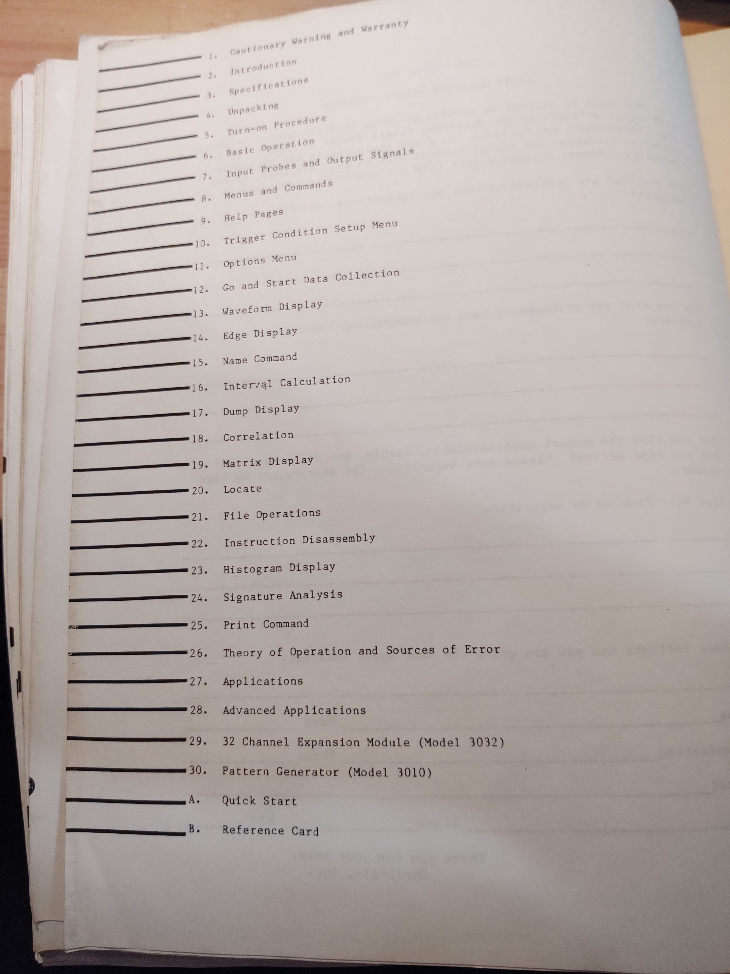
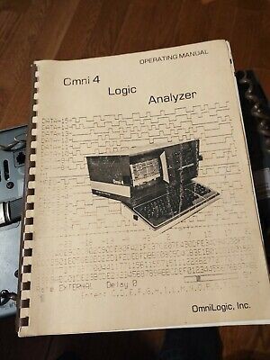
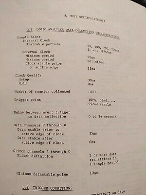
Dominic--who happens to be selling the only other OMNI4 I'm aware of in existence--very kindly scanned and sent me the user manual [possibly the only in existence] for posterity!
A copy is in the Files section.
BTW, Dominic's been quite awesome taking the time to do this and more. If you're intrigued by the OMNI 4, consider purchasing it from him at:
If you decide to purchase this unit, please keep in touch, and consider joining the 'team' here to contribute!
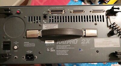
This unit differs from mine in at least one notable way; mine doesn't say anywhere on it that it's a Kaypro 2x. @ziggurat29 had to figure this out by looking up Kaypro motherboards!
[Also, an odd note, apparently when using 'cpmtools', one must select 'kpiv', even though the Kaypro IV is an entirely different beast(?)]
[TODO: take similar shots of mine for side-by-side.]
This appears to have the drop-down door type latch floppy drives, whereas mine has the rotating lever-latch.
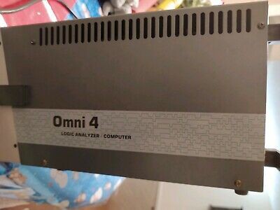
A manual!
"Kaypro 2x" heh, that'd've been handy
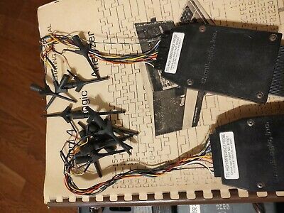
Hmmm, my pods are merely heatshrunk, and their cables merely ribbon cables. [And, crosstalk/interference was an issue]. Seems even more plausible, now, mine might've been a prototype?
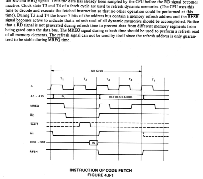
So, the question, earlier, came up regarding how the DRAM gets refreshed, if the /REFRESH pin is N/C (which it appears to be, according to the schematic).
and dammit if I didn't have a long write-up on the matter, and lost everything after this point. So, I guess I'll get to the point.
There's really no *need* for the /RFSH signal. At least with typical DRAMs. Basically, a row in the DRAM is refreshed whenever a row is accessed. And for a typical Read/Write operation, the row is accessed first, then the column, then the Read/Write signal is sent. So, the row gets refreshed with every read/write access.
So, why not treat *every* address placed on the address-bus, accompanied by /MREQ, as a Row AND Col access, as though for a read/write? And... now I'm pretty sure that's what happens.
Simple. And I'm betting the custom chip doesn't contain any specialized logic regarding refresh.
----------
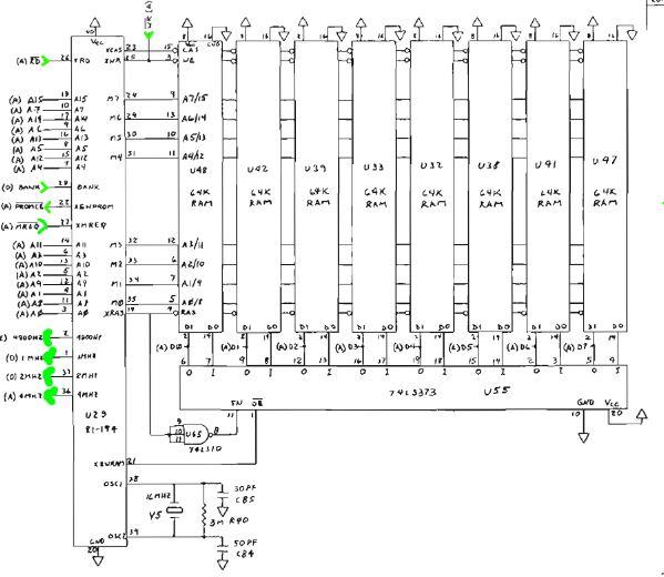
There's still the issues of BANK and /PROMCS, and how those are related to the DRAM... My guess, again, is that *every* address-access on the Z80's address-bus, accompanied by /MREQ, accesses a memory-location in the DRAM (even, for instance, when the ROM is being read).
BANK is controlled by a bit on the "system port" register... That, as we understand, chooses whether to do memory-accesses from the ROM or the RAM. So, e.g. during boot, BANK directs it to the ROM, then after boot, its directed to the RAM where the OS is stored, etc. (There's some debate as to whether the "BIOS" in the ROM is accessible to applications once the bank has been switched to RAM... E.G. if there could be, say, routines in the BIOS for displaying characters on the screen, could that be called from a user-application, switching into the ROM for execution, then back into the RAM for the next portion of the user-application? I'm sure there are ways, but they may not be pretty... e.g. storing *pieces* of the same code in both ROM and RAM, at the same locations... I'm sure I can find out with further analysis of Ziggurat's ROM disassembly).
So, obviously, when BANK is set to ROM, /PROMCS gets activated with /MREQ, but /XENRAM does not. But, then, when the ROM is executing (during boot), the RAM still needs to be refreshed... so its still feeding *every* address-access to the row/col system... Which is fine for /RD, since /XENRAM is disabled and therefore the data in the DRAM is not written to the data-bus...
But what about Write...? /WR is not gated through the custom chip, it goes *straight* to the DRAM!
Ah hah!
Write... Never Happens to the Read ONLY Memory.
OK-then...
Now this leads me to the question of how the ROM can access RAM, for storing variables, etc.
In what I've seen of Ziggurat29's disassembly, it seems the stack-pointer is set-up in a high-address, e.g. 0xff00... and it seems most other variables are stored up there, as well...
So, then, BANK only switches between ROM and RAM in the *lower* addresses, and always accesses RAM in the higher ones... simple enough.
And, again, by treating the RAM as though it's being accessed even when the ROM is, but gating the RAM's /RD signal (/XENRAM), it still gets refreshed.
This custom chip is starting to seem quite simple, really... a few gates.
(As Ziggurat29 pointed out a while-back, the 2x motherboard uses this custom chip, but the earlier motherboards are similar in design but use discrete logic instead... I've been meaning to look at those, but haven't yet. All these ramblings are from the perspective of treating it like a black-box... I guess it's kinda like doing math homework where the answers are in the back of the book... should I go look?)
-----------
Whoa Whoa Whoa!!!
that /WR signal is *directly* connected to the DRAM chips! And they don't have Chip-Selects! That's fine for ROM... but...
What the heck happens during an I/O write!?
... "/CAS is used as a chip select activating the column decoder and the input and output buffers."
So, maybe I'm mistaken in the above assumptions that /RAS and /CAS are *always* strobed... Maybe only /RAS is, and /CAS is only strobed alongside /MREQ... oy!
-------
I do, in fact, have a logic-analyzer occupying *exactly* the same space as the circuit I'm curious about... And that logic-analyzer, in fact, samples quite a bit faster than the circuit I'm curious about... THAT would be the logical approach.
------
This looks quite handy, though I think it's for a KayPro 2, rather than 2x...
1) An image-search for '"Omni 4" "Logic Analyzer"' results in many hits from this project-page... pretty cool. OTOH, it's quite strange, saying that many of the images are "4-5 days ago" that were actually several months ago. (is it 4-5 days ago that Google crawled on 'em?)
2) A resulting-image doesn't show anything related to the OMNI4... so I clicked through to the page to see what Google thought made it relevant... Apparently MAME now comes with the OMNI4 ROM (?!)
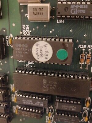
(Note that we've determined the motherboard is a pretty-much stock KayPro 2x, but it has a custom Boot-ROM and Character-ROM, both of which are available in the "Files" section of this project).
Herein, I'm gonna throw up some notes, as I read-through his work...
(Note that I currently have Zero experience with Z80 assembly-language, and am pretty slow with assembly-language in general, and am unfamiliar with the unit's registers/peripherals... So, this is a great learning-opportunity. Interestingly, this is the same approach I took in learning about the IBM PC/XT architecture, by looking at the BIOS Assembly-listings and schematics in order to determine how to initialize and make use of its peripherals.)
You might want to take a look at the KayPro Service Manual, which contains schematics of the KayPro 2x motherboard.
-------
First interesting note...
The BootROM appears to launch right into external (to the Z80 chip) register-setup... Apparently not much configuration needs to be done within the Z80 CPU, itself.
There is a "system port" register at 0x14 consisting of quite-literally a byte's worth of TTL Flip-Flops whose outputs are fed to various peripherals, most-notably the Floppy-Controller, but also the Character-Generator ROM (and more?). Setting up the "system port" register is the second operation, the first being setting up the stack-pointer, and both are accomplished in only a small handful of instructions. Wild.
UPDATE: The system port (address 0x14), from the schematic:
(Side-Note: Appears that the parallel-printer port is output-only, and reading the written values is not possible... wouldn't take much modification to make it bidir... strap a '244 atop that '373, and some glue...)
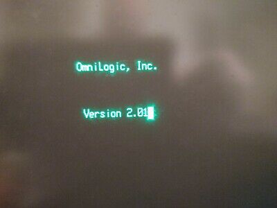
Immediately thereafter, is the version-string "2.01", which gets loaded into RAM. This version-string appears on several screens... E.G. When the unit is turned on, as I recall, it says something like "Omni 4 version 2.01" and also, upon loading CP/M, something like "Omni 4 CP/M version 2.01". (TODO: verify... I thought we had CP/M 2.2..?)
It's interesting to me that these two things are in the Boot-ROM, as I'd've thought CP/M was loaded from the disk (and therefore its version would be dependent on that which was on the disk... like, e.g. DOS 3.3 vs. DOS 6... Or Windows XP vs. Windows 10).
(To-Ponder... The RAM is already being filled with data, including the version-string and the stack, at this point... More, surely, to come... But doesn't this system use DRAM? Doesn't it need refreshing? How about column vs. row-addressing? Is that *all* handled via dedicated circuitry?! (UPDATE: Looking at the schematic, it appears U29, a custom chip numbered 81-194, takes care of this. This chip appears to handle only interfacing with the DRAM and generating a few clock-signals, from 4.9KHz to 4MHz. As (Actually, it has a couple other outputs I'm working out). Ziggurat29 has pointed-out, this custom chip is a new thing as of the '84 versions of KayPro systems like the 2x, the prior versions used discrete logic, which I've yet to look into. Interesting that, at the time, designing and manufacturing a custom 40-pin chip is cheaper than just replacing the DRAM with a 64K SRAM). (An aside: I began looking at the Z80 timing charts, earlier, and noted that there's a "refresh" portion of *every* instruction-fetch bus-transaction... haven't wrapped my head around that one yet... UPDATE: Apparently the /REFRESH output on the Z80 is N/C... hmmmm.... more at the bottom).)
-----
Next comes the bit I, personally, would be most-interested in attacking as quickly-as-possible, and here it is, being attacked as quickly-as-possible... initializing the video-system.
It appears to load 16 values to 16 registers in the video-controller IC... These values are hard-coded in the ROM... And the procedure for writing these registers appears to be to load address 0x1C with a register-select value (0x00-0x0f), then to load address 0x1D with the new value for the selected register... repeat 16 times.
Ziggurat29 notes that apparently register 0x1f is selected (but never loaded with a value?). This, apparently, is not a register on the video-controller IC... Not sure what it does... (Maybe it's a method to assure that should address 0x1D be written, later, it won't accidentally overwrite whatever last-register was selected?)
And, from there a handful of other operations, and... initialization of the video subsystem doesn't seem to be particularly-difficult. And, maybe more importantly, getting to the point of actually displaying a character on the screen is on the order of maybe 100 lines of assembly (maybe 20-50 lines of C code). Not bad, considering that's from the moment of power-up...
E.G. for the PC/XT, in my previous project, to display a character on the CGA card... Well, weeding out what was necessary to do-so from the BIOS listing was quite an ordeal... As I recall, there was easily 200 lines of (executed) assembly just to get to the point of initializing the CGA card, including things like setting up the DMA controller to refresh the DRAM, setting up the floppy controller, interrupts, and quite a bit more that technically aren't necessary for interaction with the video-card. Further, the PC/XT BIOS can handle several different types of video cards (including none), so a significant amount of the code determines (repeatedly!) which card is installed, and more. In the end, maybe it would've taken roughly the same amount of configuration (~100 lines of assembly) to get the PC/XT's video-card running, as the KayPro's, (if you know which card is installed).
(UPDATE: It appears that the Z80's /BUSRQ and /BUSACK pins are unused... No DMA here! This'll certainly make a brain-transplant easier)
.....
Maybe this analysis seems like a strange approach... Well, what if you were writing your own custom ROM just for the sake of learning the system... Wouldn't the first thing you'd want to do be to make something blink? Here, the KayPro (or at least the OMNI4) BIOS apparently does exactly that as pretty much its first priority.
(In my PC/XT project, my goal was to replace the original 8088 chip with one I'm more familiar... an AVR, yahknow, basically an Arduino. That way, among other things, I could use my normal coding-habits to work with the PC/XT's motherboard/peripherals, rather than learning a new language (x86 assembly)... Here, it looks like substituting the Z80 CPU on a KayPro with, say, an AVR, and making use of the KayPro hardware may be *significantly* easier than on a IBM PC/XT... so may be a great learning-platform. (I never did get to interrupts or DMA on the PC/XT).
The big hurdle, still, will be making that AVR compatible with the Z80's bus... Doable, certainly.
(Oh, and, in no way is this suggesting to run the old KayPro's software on an AVR... this is about coming up with your own software to work with the hardware-level stuff... why? I dunno. But, yes, I'm willing to bet an AVR, cleverly-coded, could emulate a Z80, and possibly even execute instructions at roughly the same speed, maybe faster).
--------
I got a bit side-tracked... And I'm stopping, here, with video-initialization, for now.
Please look at the *comments-sections* of the previous logs on this project... Ziggurat29 is apparently brilliant, but has a habit of posting what could be entire log-entries in the comments-sections of my otherwise bland log-entries. That is to say, you can learn a *lot* by scouring in deep dark recesses of this project-page for his comments!
Some highlights from the previous log's comments include a memory-map, and explanation of the interrupt-system. Also, apparently the BIOS ROM shares the same memory-space as the RAM, so when an application is loaded into RAM, the BIOS is effectively removed from the system (?!). Ziggurat29 goes into some detail as to how that may function. Also, it seems he's done quite a bit in disassembling higher-level things such as the operating-system, which I'm obviously a ways from analyzing.
----
A couple other notables upon browsing the schematics...
There appears to be a header for a light-pen. And apparently building one isn't too difficult. So... oy... I had one once, long before I knew how to program... and had no idea where to connect it on my old PC, so I never was able to use it, and managed losing it. But apparently they're pretty easy to make... and now I know a bit about programming... So an easy distraction to ponder. Though, I could do that just as easily with the PC/XT... and haven't yet. It's kinda curious, here, since this system doesn't do graphics (without some hackery).
----
The I/O ports are addressed with A2-7, leaving A0 and A1... not exactly unconnected, but almost. E.G. the "system port" D-latch chip is selected by 0x14, that's A4 and A2 high (the rest low). But, since the selection-circuitry doesn't make use of A0 and A1, I'm pretty certain the system port could just as easily be accessed at 0x15, 0x16, and 0x17, as well... The result would be the same.
At first this didn't make sense to me... wasting all those I/O addresses... But now I see, I think some other devices, themselves, make use of A0 (and possibly A1). E.G. the video-circuitry... So e.g. the video-chip's chip-enable is selected by A7-A2 = 0x1C, but then it's also selected when the address A7-A0 is 0x1C, 0x1D, 0x1E, and 0x1F. Its internal registers are chosen with A0/[A1], thus, we have different address-selections on the video card for 0x1C (register-select) and 0x1D (register-value). (Not sure, yet, whether it also makes use of A1 for other registers). Makes sense, and now that I've traced most of that out in the schematic seems totally obvious (haven't I seen the likes of this on other systems... for like... decades now?).
I guess the difference, here, is that the motherboard contains decoders for *all* the I/O devices (onboard, anyhow). Whereas, say, for a PC/XT, each ISA card has its own address-decoder circuitry... That's a lot of duplicate circuitry for a serial port, a parallel port, a floppy controller, a video-card, an RTC, etc. (I suppose why those multi-function cards became so popular, and eventually became a single chip).
Whereas on here, most of those devices are onboard, at fixed addresses, and therefore one set of address-decoder-chips (only two 3-to-8 demultiplexers) can select all those I/O devices.
Apparently pip decided to translate tabs to spaces.... even in binaries, even in binary mode.
On that note... cpmtools seems to work with the disk image when using the kpiv format.
Only one hiccup (besides discovering the tab to space conversion)... a large text file ends with a bunch of 0x1a's... (ascii substitute?) Dunno why, but doubtful they belong there.
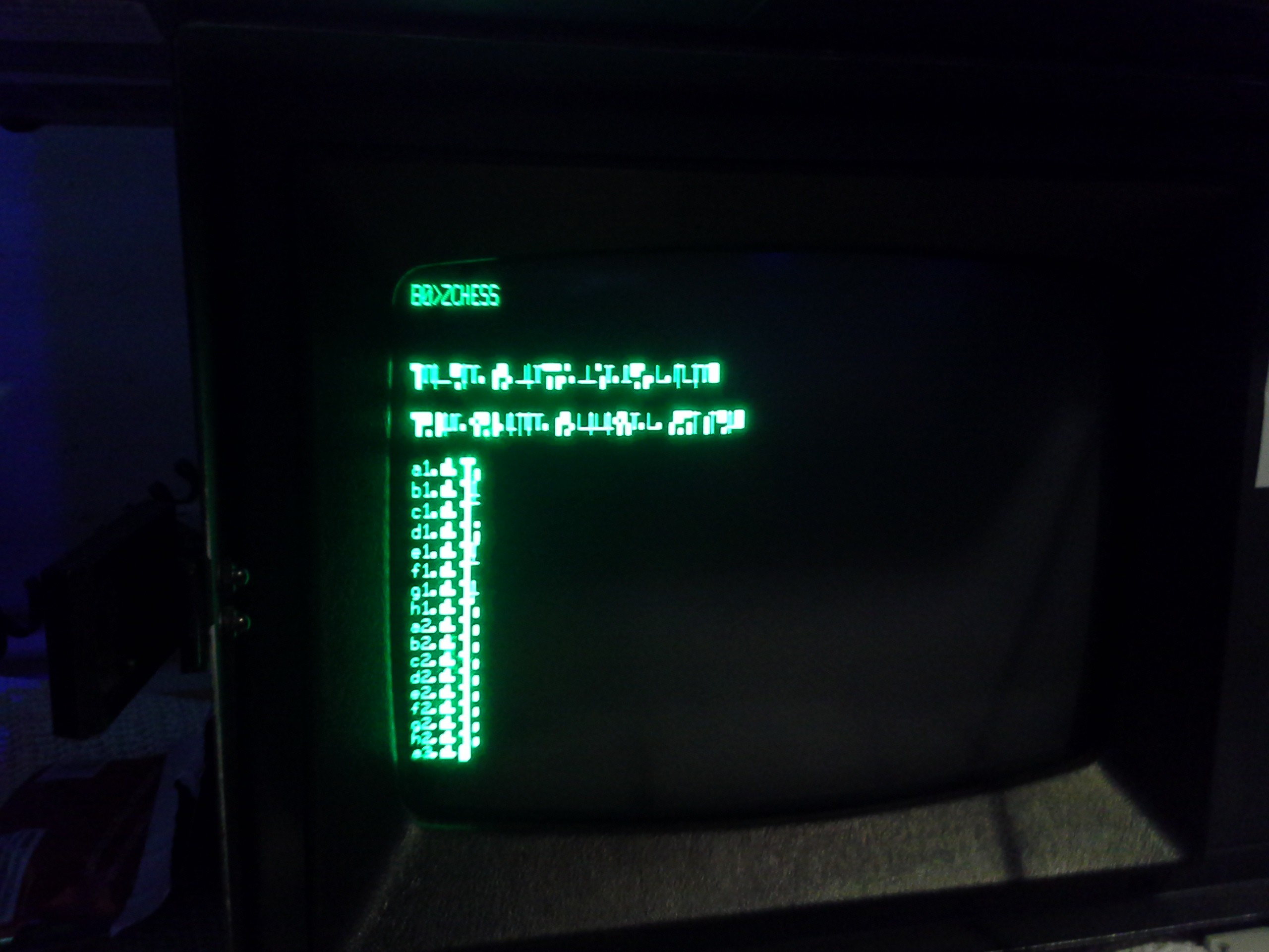
u9 appears to be the character ROM... there's a 2732 24 pin EPROM in the socket. Its contents is in the files section, and ziggurat29 decoded it into ascii art. It appears the Omni4 has a custom character set for drawing logic waveforms.
Ziggurat noted that the schematic shows pin 2, a12 is driven from somewhere... (where?). Well the 2732 doesn't have an a12, but the 2764 does... and the 2732 is pin-compatible-enough that it could be dropped in a 2764 socket, if said socket is designed with that intent... which this one is. And that explains the larger socket than the chip...
Ziggurat also noted some code in the bios that seems to support character-set switching (via a12, most likely)...
So my guess is that this was designed with the intent to support two character sets... a normal one for normal stuff... and switching to the custom one for the logic analyzer.
Seems logical.
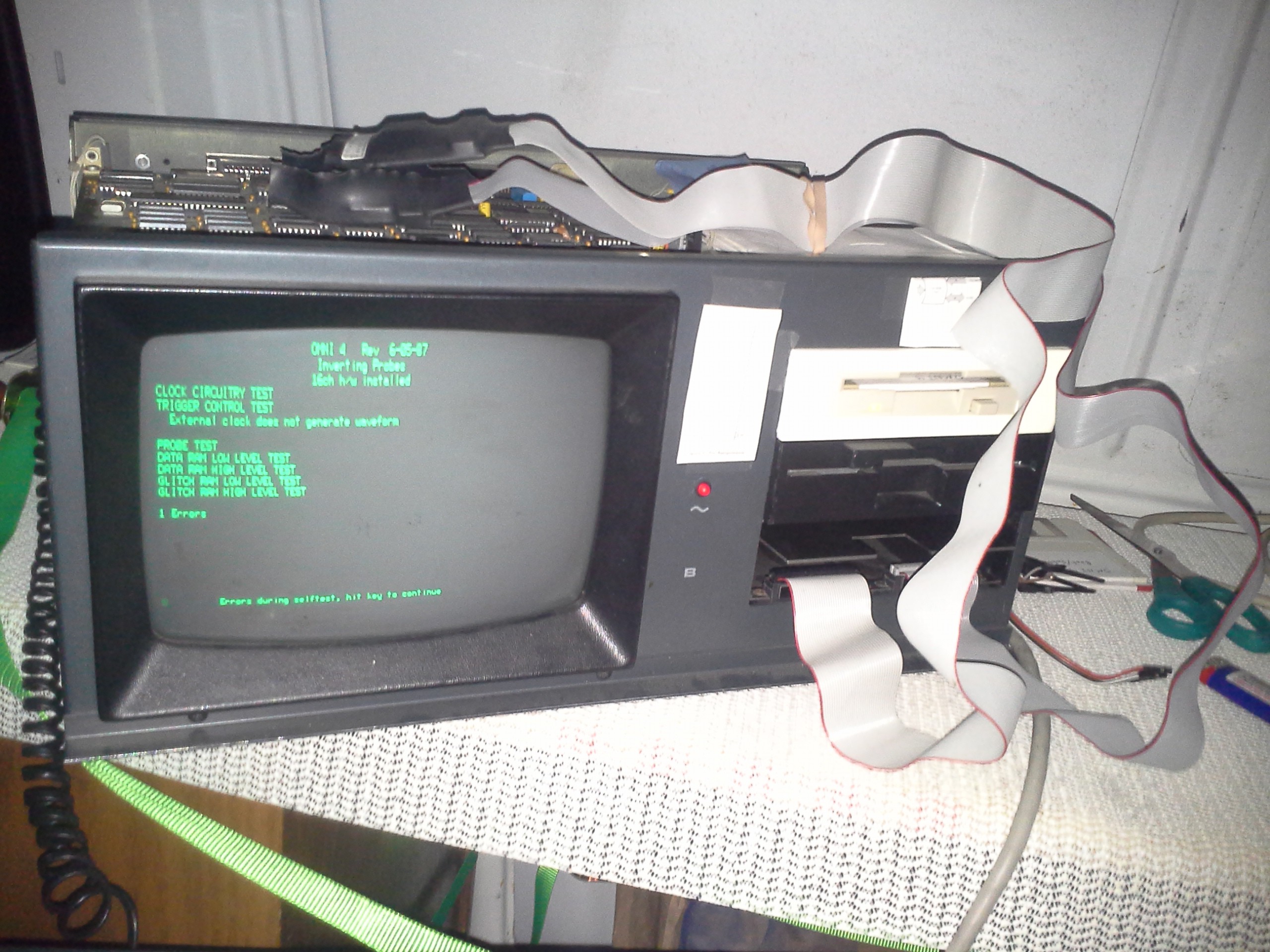
So some tests run tonight:
A12 starts low, upon reset, but goes (and stays) high as soon as the boot title screen pops up... even before the disk is read, so before the os is loaded, and long before the logic analyzer software is loaded...
This seems backwards to me... certainly itit'd be more logical to use the default character set for boot, then switch charsets when loading la.com...
An easy change... for a designer... and another thing leading me to think this guy's a prototype (or they ran out of energy for such a simple change... with the assumption few people would be using a $4000 logic analyzer to play games?). While the change would be simple, it would require modifying both the bios and la.com (and any other related software)... so I can see how a backburner idea like that might've been abandoned...
So... since a12 isn't used on the 2732, and since the 2732 only contains the custom charset, the machine thinks its accessing the custom charset (immediately upon boot and always thereafter) in the higher address space of a 2764... but it's really wrapping around and accessing the lower address space, which is fit in a 2732.
So I guess... if this were something I cared to fix, like if i wanted to play games on this thing, I could load the custom charset in the higher addresses of a 2764 and the regular one in the lower space, as designed... then I'd need a utility to switch to the normal charset every time I wanted to play a game... which would mean not being able to just boot off any floppy.
Or... I could swap it from the presumed-intended design... have the custom charset in the low space and the normal one in the high space... this'd mean having a utility run before the la software to switch to the low space. Could do that in some sorta script, right?.. completely goofy, but a solution that would allow normal disks to boot with the normal charset.
Now... what if there are games, etc. That expect their own custom charset..? Or, maybe weirder, what if some programs reset to the default charset when starting... Who knows.
It definitely looks, though, as if this charset swapping is a thing designed in kaypro 2x's... not limited to the omni 4... but am guessing the choice to set a12 high in the bios is specific to the omni4...
Anyhow, a curiosity.
.....
Probing: A12CH appears to be connected to U58, PIN 16... heading back to the schematic... yep... there it is, sheet D just as it says... dunno how I missed it before.
.....
Replaced the second 5.25in drive with another 3.5... MUCH easier, now, to try out other software... (looking into something that'll transfer the disk contents faster and reliably for viewing on a newer computer).
Not sure where I stand with this thing... I'm starting to get hackish ideas... that can't end well... and... could be done with a normal kaypro, anyhow...
(Seriously: installing a soundblaster has crossed my mind a couple times... maybe I'd better get this thing out of my sight ASAP... I can do stuff like that with #Improbable AVR -> 8088 substitution for PC/XT instead of frankensteining one of the last of an endangered species)
...
Also... found a disk image online containing ebasic.com... yep. BASIC. so now can twiddle some bits... tried to read the RTC... it thinks it's April 1989. Spose it's possible it wrapped there after y2k... the time's way off. Otoh, no idea whether it was set in this time zone (or at all)... and I'm betting thirty minutes in either direction could easily been lost/gained in thirty years... thing is, the 3v battery still reads 2.7v... so it's probably still trying to keep time. But it seems funny these things even have RTCs... 'cause I haven't found any software that reads it, and certainly none to set it!
Note that the end-result is very different than a null-modem... weird world.
(CTS <- DTR, NOT CTS <- RTS, was necessary, otherwise the transfer never starts)
Truns out pip doesn't convert *to* ihex, only *from*... well that doesn't help. OTOH, looks like the serial port does infact send 8 bits.
On the PC-side I used 'dd bs=1 if=/dev/ttyUSB0 of=<filename>' (after setting the baud-rate to 300bps (!!!))
On the KayPro side I used 'pip tty:=<file>[o]'
tty: is the serial printer port, and [o] indicates to send the file as binary, so it won't stop early when a byte matching 'end-of-file' is found.
After the transfer completes, the KayPro returns to 'A>'... at which point I type <CTRL>-C on the PC.
The process is *slow*... and pip doesn't say much while it's running... or not (e.g. when the handhaking is not correct, it just stalls... forever?)
So I opened another terminal window on the PC and ran 'ls -l <filename>' repeatedly to make sure that filesize was increasing.
Many files from the disk are now available in the files section, after literally hours of file-transfers ;)
.......
There were some strangenesses during the transfers. I transferred K2X* twice, and verified they matched. LA.COM I transferred numerous times and verified they matched, but the remaining I did not verify. Oddly, unlike the others, their file-sizes didn't match the output of 'D.COM' (which is essentially 'dir' or 'ls'). One I tried twice, both times receiving 4K, when D.COM claimed it was 6K... so I dunno.
 Eric Hertz