 Bud Bennett
My first attempt at a differential oscilloscope probe was over five years ago. Its progress is documented as “A 10X 100MHz Differential Probe” here on Hackaday. It’s time for an update. I was impressed with the design modifications that Chistoph and Wolfgang pursued, but apparently never finished, so I recently decided to continue on with their initial ideas for improvement, but make it generally more useful for the DIY community rather than those with the wherewithal to have a Keysight Oscilloscope. If you have a Keysight scope, here's your probe (only $1900).
Paul built a 100MHz probe and a 10MHz probe. He published his notes and measurement results here.
Changes:
- A slimmer layout. Roughly 13mm x 100mm, making it less blocky and more probe-like. The longer probe will also make it easier to hold and handle while manually probing around circuits.
- Modular. The previous design had two incarnations — mine and Paul’s. Mine was powered by an isolated 5V wall adapter. Paul’s power was a 7.5V-12V wall adapter, which required an on-board voltage regulator on the probe. This new probe uses a basic core probe that requires 5VDC, or 15VDC isolated power, but it can be configured to accept various USB connectors and voltage ranges through the use of separate daughter boards that plug into the rear of the probe’s core PCB. Right now there are 5 daughter boards: a standard micro USB-B 5V interface, three voltage regulators that will take 7.5V-12V (bare wires) as an input and deliver 5.3VDC to the probe, and a USB-C trigger board that provides 9V or 12V to the voltage regulator daughter board. Something for everybody. The daughter boards are small, and therefore relatively cheap, made with easy to get ubiquitous components. Beware, the reverse polarity protection has been removed.
- [2025-07-08] Added two lower bandwidth versions: 10MHz and 1MHz. Both versions have increased differential input voltage range (140Vpp). These versions require a 15VDC power source, which is easily available from a USB trigger board.
- A power indicator LED. Meh.
- Offset adjustment. Up to 35mV of adjustment to the output voltage of the probe. This is not without some degradation in performance — both gain accuracy and supply rejection, along with other untoward negativities. But it is optional if you decide it is not worth it.
- Improved common mode rejection at higher frequencies.
- A 3D printed case, which should allow for reduced sensitivity to external EMI if shielded with some copper tape.
100MHz Probe Specifications (haven't changed from the older version):
- Input impedance: 20MegΩ// 1.25pF - differential, 10MegΩ//2.5pF each terminal to GND.
- Differential Gain = 1/10 V/V. Any lower than this and the DS1102E could not resolve a 1V signal with any clarity. (Many of the cheaper differential probes are switchable between 50X and 500X attenuation. This would be good if the signals in which you are interested are very large, but that's not the case so far with my needs. The better probes ($400 and up) provide 10X/100X attenuation.
- Max AC Common Mode Voltage (with 50Vpp differential input voltage) = 350VAC
- CMRR >90dB @ DC, ~60dB @ 1MHz
- Differential Voltage Range > ±25V for 240VAC common-mode, ±25V for 0V common-mode
- 3dB bandwidth ≥ 100MHz (Dependent upon signal amplitude)
- DC offset < 1mV (trimmed)
- Noise: 200-300mVpp input referred.
- Input power: 5-5.5VDC @ 60mA.
- Cost: ~ $50-$60
The 100MHz Probe Schematic:
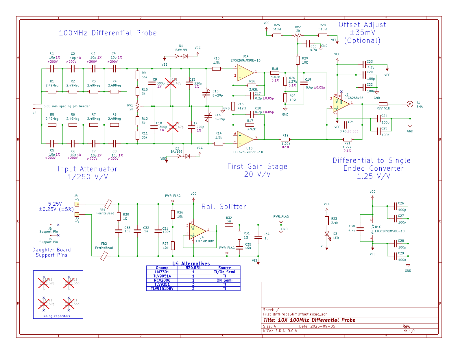
No surprises here. This design was described in gory detail. See the old project.
Electrically, it is nearly identical to the previous design. C1-C4 now connect across to R1-R4 because all of the R's and C's are the same value. Paul added the 4 tuning capacitors so that they would appear on the BOM. C15-C16 were changed to a JR300 trimmer (or cheaper alternative), doubling the trim range with the tradeoff of poorer temperature variation. There are fewer bypass capacitors at the splitter output. FB3 was changed to R32, a 3 Ohm resistor instead of a ferrite bead, to prevent oscillation in U4. I changed the tantalum tank caps to ceramic and added a discrete snubber resistor -- it's too difficult to find a small tantalum with the correct ESR. A power indicator LED was added. C19 was added to improve CMRR at higher frequencies. Note that the schematic doesn't include any power supply options -- those are provided by the various daughter boards.
Users complained about the cost of the LM7301 opamp. There is a list of possible alternatives.
10MHz Probe Specifications:
- Input impedance: 10MegΩ// 2.5pF - differential, 5MegΩ//5pF each input to GND.
- Differential Gain = 1/10 V/V.
- Max AC Common Mode Voltage (with 140Vpp differential input voltage) = 350VAC
- Max input voltage = ±600VDC or 424Vrms
- CMRR >85 dB @ DC, ~50 dB @ 1MHz
- Differential Voltage Range > ±70V for 240VAC common-mode, ±70V for 0V common-mode.
- 3dB Bandwidth ≥ 10MHz (for Vin < 60 Vpp). Slew rate limited.
- DC offset < 1mV (Trimmed)
- Noise: 1.5mVrms (20-30mVpp) input referred.
- Power Input: 15V ±0.5V. This can be from an adapter or from a USB-C trigger board and daughter board combination.
- Cost: ~ $30.
10MHz Probe Schematic:
Uses the same PCB as 100MHz probe. Different amplifiers and attenuation/gain parameters.

The 100MHz probe has about 250mVpp of noise wrt its input. This makes it difficult to resolve small excursions unless you have an external trigger and waveform averaging employed on your scope. This probe should have 10X lower noise. For what I do mostly, 10MHz BW is good enough.
The input resistance was lowered from 20MegΩ to 10MegΩ and the capacitance was raised to 5pF, which should make the probe look like a standard 10X probe with 10MegΩ/15pF input specs. The higher supply voltage allowed the attenuator to drop from 1/250 to 1/100. The first gain stage was lowered to 5 to hit the 10MHz BW target, at the expense of slightly poorer noise performance. Bypass capacitor values and voltage ratings changed to accommodate the higher supply voltage.
The 1MHz Probe Specifications:
- Input impedance: 10MegΩ// 2.5pF - differential, 5MegΩ//5pF each input to GND.
- Differential Gain = 1/10 V/V.
- Max AC Common Mode Voltage (with 140Vpp differential input voltage) = 270VAC
- Max input voltage = ±600VDC or 424Vrms
- CMRR >85 dB @ DC, ~50 dB @ 100kHz
- Differential Voltage Range > ±70V for 240VAC common-mode, ±70V for 0V common-mode.
- Bandwidth ≥ 1MHz.
- DC offset < 1mV (Trimmed)
- Noise: 0.5mVrms (3mVpp?) input referred.
- Power Input: 15V ±0.5V. This can be from an adapter or from a USB-C trigger board and daughter board combination.
- Cost: ~ $30 (same as 10MHz probe.)
The 1MHz Probe Schematic:
Uses the same PCB as 100MHz probe. Different amplifiers, attenuation and gain parameters.

The input referred noise of this probe is expected to be less than 3mVpp. I think this will produce a nice thin trace on the scope even for 10mV amplitude (10mVpp) signals. The design is pretty much the same as the 10MHz probe, except that the first gain stage was increased to 8 to suppress the input referred noise a bit. All of the filtering is performed by the last stage to get rid of as many forward noise terms as possible.
The Layout:
Consists of a long, skinny core. All of the different bandwidth versions use this same PCB.


- Initially, I just copied Christoph's layout (and the laziness of the 3-pin header at the input), but quickly found out that 13mm is near the minimum width considering the spacing required by the protection diodes and trimmer capacitors. The PCB is longer to accommodate the offset trim and daughter board at the back. Some components are mounted at the back -- I used smaller 0402 capacitors to take up less room and have a lower height.
- The 13x13mm daughter boards are soldered onto the back side, using the pin headers that fit a 1mm hole diameter. Pin spacing is 10.3mm. There is just enough room for a few components and/or USB/other connector. More on that later.
- There are three mounting holes to secure the case halves. There's not a lot of room, so M2 screws are used.
- The distance between the input pins is widened, supposedly to prevent stress or creep from the high voltages. But I'm having my doubts, given that the input voltage differential should always be less than 70V in normal operation. It's the common mode voltages that are high, not the voltage between the inputs.
- I eased up on a lot my paranoia surrounding high frequency design. Symmetry is still required, but massive traces and power/ground planes I think not (but I might be wrong).
- I just slapped that micro-strip between R22 and the SMA connector, using an online app that gave me close to 50Ω impedance. I'm not sure that it matters much, given that the scope interface is not 50Ω, but the coax pigtail impedance is 50Ω so it is better to avoid unwanted reflections.
Daughter Boards:
Most people won't cut the connector off the end of a wall adapter and dedicate it to this probe like I did. There are lots of power adapter plugs out there, so we made the power interface modular to accommodate that. These PCBs are small, and relatively cheap ($1.30 for 3 pcs from OSH Park.) Right now, there are six different daughter boards (so far):
Micro USB (or USB-B)

Nothing here but a micro USB jack mounted on a 13x13mm PCB with pin headers soldered in the corners. This assembly gets mounted onto the probe like so:

The daughter board should be mounted TBD distance away below the probe PCB to accommodate the spacing required between the SMA connector and the micro USB connector.
Voltage Regulator Daughter Board:
The voltage regulator that we chose for Paul's probe became difficult to procure. I decided to remove that obstacle this time around and designed a very simple regulator using ubiquitous components that are available from multiple sources.

U1 is a TL431 shunt regulator that has been around forever and is used in just about every wall adapter supply on the planet. There are many many suppliers, and it's pretty cheap. It comes in three tolerance grades -- 0.5%, 1% and 2%. A quick search of Digikey shows six suppliers offering prices starting below $0.12 in low quantities. Same for the two BJTs, which are needed to share the power dissipation when the input voltage is at 12VDC. (See the project log for all of the details on this circuit.) It all fits onto the 13x13mm daughter board:

There is no connector provided. Barrel jacks are just too big (5x2.1mm won't fit on this tiny board.) You could mount a 2.35x0.7mm barrel jack, but good luck finding an adapter with a matching plug -- they all use the larger 5x2.1 size and provide an adapter that is too large to put next to the SMA cable and hang off the end of the probe. We decided to just provide solder connections and leave it up to the user to decide what to do.
This daughter board is mounted the same way -- underneath at the required distance. The components are mounted on the underside of this PCB in order to accommodate the USB-C trigger board.
USB-C Trigger Board:
The USB-C interface can provide various voltages (5-20VDC) from a conforming power adapter, but require some intelligence to do so. You need a USB-C trigger board to take advantage of those voltages. Trigger boards are available from various suppliers (including Amazon), are cheap and small. They are probably cheaper than you could build your own.

The trigger board shown above is the maximum length that will fit inside the case. There are smaller trigger boards available, but they have only two voltage options: either 9/12V or 15/20V. The voltage can be changed by adding/removing a small (0402) shorting resistor or solder bridge (upper right).

These trigger boards can be stacked (glued?) below the VREG daughter board to provide a USB-C interface and a regulated 5.3VDC or 15VDC to the probe. That is why the components on the VREG daughter board are mounted underneath. Here's what that looks like:

Easy peesy.
SOT89 Daughter Board:
This is the same LDO that was used on Paul's version of the probe. This XC6716 might be hard to get and might not be the best LDO to use for this application now.

It should be good for 7.5 < VIN < 12V.

The SOIC8 Daughter Board:
The LP2951 might be cheaper and easier to get. [2025-10-21] I changed C1 and R4 to provide a snubber effect for any connected USB-C power supply. This should suppress spikes associated with the switching converter in the adapter. It might not be enough, but I tried.

The SOIC8 fits nicely.

Note that the SOIC is shifted far to the right. That's to avoid pins touching the SMA connector's housing.
The Buck Converter Daughter Board:
I started this just for fun, but I think this is probably the best approach to get the lowest power dissipation and heat. It is also pretty cheap.


The Case:
I never built a case for the previous probe. Users complained that the probe was sensitive to external interference. Now I have a 3D printer and should be able to design something that works. Wrapping copper tape around the front of the case provides better shielding.

This is my best shot so far. I'm no expert at 3D modeling so this was a very long exasperating experience in FreeCAD 1.0.
The lid exterior/interior:


There are holes in the lid to access the trims and internal supports for the PCB. The PCB fits in the shoulder. I expect to use self-tapping screws to hold the case halves together -- no nuts.
The case bottom exterior/interior:


The Bad Stuff:
If you read this far down, then you're probably interested in building one of these. There are some things you should know first.
- This is definitely a DIY project. C11 and C12 are depopulated for a reason -- their values will probably be different for your board. The capacitors in the attenuator are fairly low values and subject to parasitic errors (even though they are specified to be 1% tolerance.) Bud found them to have an effective value 7.5% below specified. C11-C12 will probably need to change to accommodate this error. It's not a biggie, but it's a big tell that this is not really a production ready product. And that's OK.
- It will be difficult to obtain all of the components. You will probably be required to make substitutions. You should make sure that your substitution is really equivalent to the original component called out in the BOM. There are a few components that don't matter that much. In those cases, for example, if I've specified a tolerance of ±5%, but the source has a ±1% tolerance, you can use the wider tolerance part without issues. If there is no tolerance attached to the components properties, then it won't matter. Also, pay attention to the temperature/voltage profile of a component -- all of the capacitors are either C0G/NP0 or X5R or X7R for a reason -- don't use a Y5V component anywhere (it's not worth any cost savings.)
- The BOM is setup for the PCB to be populated by JLCPCB (only the top side). They most probably won't have all of the components in stock. You can find stocked substitutes for most of the passives, but maybe not for the trim caps or 0.1% tolerance resistors. Be prepared to solder a few components by hand if you go this route. Last I checked, JLCPCB would not place the 0.4pF 0402 caps and the trim caps, as well as any through-hole components. The cost for 5 100MHz populated, top side only, boards was $235 (no tax or shipping fee.)
- Paul and I created a list of recommended component combinations. The input attenuator can be modified to your preferences (input resistance/capacitance and/or attenuation). The layout really won't support input voltage larger than the ratings of the components. You can do what you wish, but don't blame us for the outcome.
Status:
[as of 2025-11-15] This project is completed. All of the files required to make one of these are available in the files section of the project.