 Pero
PeroCircuit design
The microwave transmitter consists of following blocks:
30 - 6000 MHz synthesizer with power amplifier
Already have an account? Log in.
To make the experience fit your profile, pick a username and tell us what interests you.
top_layer.pngTop Layer (L1)image/png - 253.94 kB - 03/30/2017 at 13:52 |
|
|
inner2.pngInner Layer 2 (L3)image/png - 181.86 kB - 03/30/2017 at 13:52 |
|
|
bottom.pngBottom Layer (L4)image/png - 166.58 kB - 03/30/2017 at 13:52 |
|
|
inner1.pngInner Layer 1 (L2)image/png - 161.47 kB - 03/30/2017 at 13:52 |
|
|
Transmitter.pdfSchematicsAdobe Portable Document Format - 229.54 kB - 03/28/2017 at 13:06 |
|
|
The obvious difference between fractional and integer mode synthesizer, is that int-mode synthesizers output frequency that is integer multiple of reference frequency, or in this case, f_PDF. Frac mode synthesizers, on the other hand can provide fraction of the step of that frequency, making it possible to generate virtually any frequency at the output.
But, improved frequency resolution is not the only advantage of frac-mode synthesizers, there is something called phase noise decrease. Phase noise increases as 20log(N), meaning that the higher output frequency will look more messy in the spectrum, to say it technically correct. If, for example reference frequency is 100 kHz, to synthesize 3 GHz at the output, we'd need N of 30000. Output divided by 4 (to 750 MHz) would look like this:
Now, if we employ frac-mode synthesizer, we wouldn't need that low reference frequency nor that large N. Instead, we could keep reference frequency at 19.2 MHz and tune the fraction. For example, in our 3 GHz example we'd need N equals 156 and additional fraction of 0.25. This fraction is defined as F/M. Given that denominator M is fixed at 100, F would be 25 and the output (again scaled to 750 MHz) would look like this:
This is improvement of almost 200 times lower N. Spectrum look much smoother and more pleasant to look at.
After verifying that MAX2871 works properly in almost every aspect I decided to write the code that will enable versatile configuration of the chip (I find it very tiring to flash the chip every time I want to update one parameter). I wrote firmware that expects user input from serial terminal to execute various functions. These are primarly PLL configurations that synthesize different output frequencies, but there are also functions to read out registers, select filters, etc.
I also wrote a Python script that provides command line interface for easier communication with the Transmitter.
Source code as well as wiki of the code is available on my Github repo.
This time, I was testing how frequency varies with user input. I wrote a program that allows user to set and change values of N and DIVA from the serial terminal. I wanted to see how can I control frequency the easiest way. But before, let's think about how is frequency synthesized in the first place.
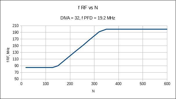
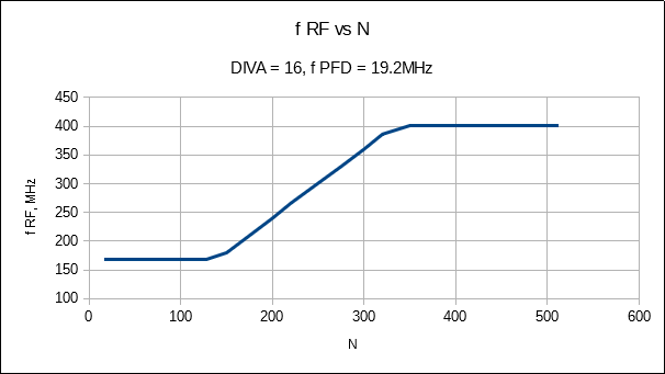
MAX2871 contains 64 VCOs organized in 4 core blocks with 16 sub bands each. I have no idea how advanced/complex in IC production is, but it surerly sounds impressive. These VCOs are able to cover any frequency between 3 and 6 GHz. The whole span is covered in steps of f_PFD, meaning that f_PFD presents max resolution of the PLL (when it is working in integer mode).
In integer mode, VCO frequency is determined as But, there is certain limit. N can not be arbitrarily chosen and the datasheet boundaries 16 - 65535 is not the only one there. Second boundary is limit of the VCOs: you can not push N f_PFD outside 3 - 6 GHz range. VCO will simply saturate and keep at limits. Another boundary comes from the loop flter. If difference f_VCO/N - f_PFD is higher than cut off frequency of the loop filter, control signal won't be applied and VCO will oscillate with lower limit value.
To demonstrate it, I've put f_PFD to 19.2 MHz (f_REF = 19.2MHz, R = 1, RDIV2 = 0, DBR = 0). I've selected output divider value DIVA to be 32 and 16 ( so I can measure it easier with my SA). Output divider determines final frequency that will be emitted out of the chip:This DIVA factor is actually the one that is responsble for such broad range: if DIVA is 128, we'll have output frequency as low as 23.5 MHz. DIVA can have 8 values, meaning that MAX2871 will synthesize frequency in 8 sub-bands.
As you can see on my schematic, loop filter is simple lowpass RC network with cutoff at 776 kHz. From above disussion, we see that it is necessary that
| f_VCO/N - f_PFD | < f_cutoff.
from there, it follows that limits for N are given by:
N_min = f_VCO,min / (f_PFD - f_cutoff) and N_max = f_VCO,max / (f_PFD - f_cutoff).
For given, settings, expected limits are 162 and 325. When N is within that limit, we can expect linear dependency of the output frequency. Outside this limits, VCO will saturate, or, stay at minimum frequency. This is exactly what you can see on the pics of measured data below.
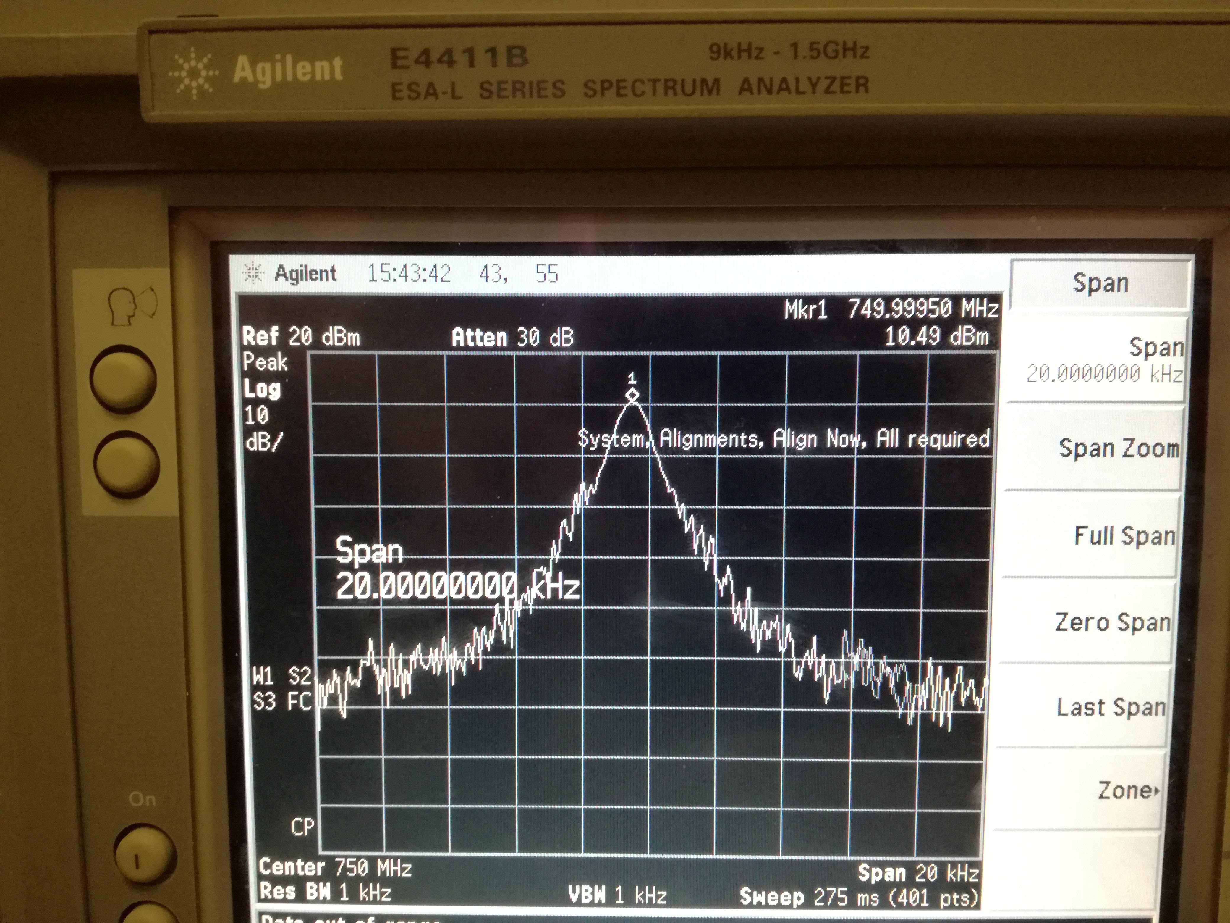
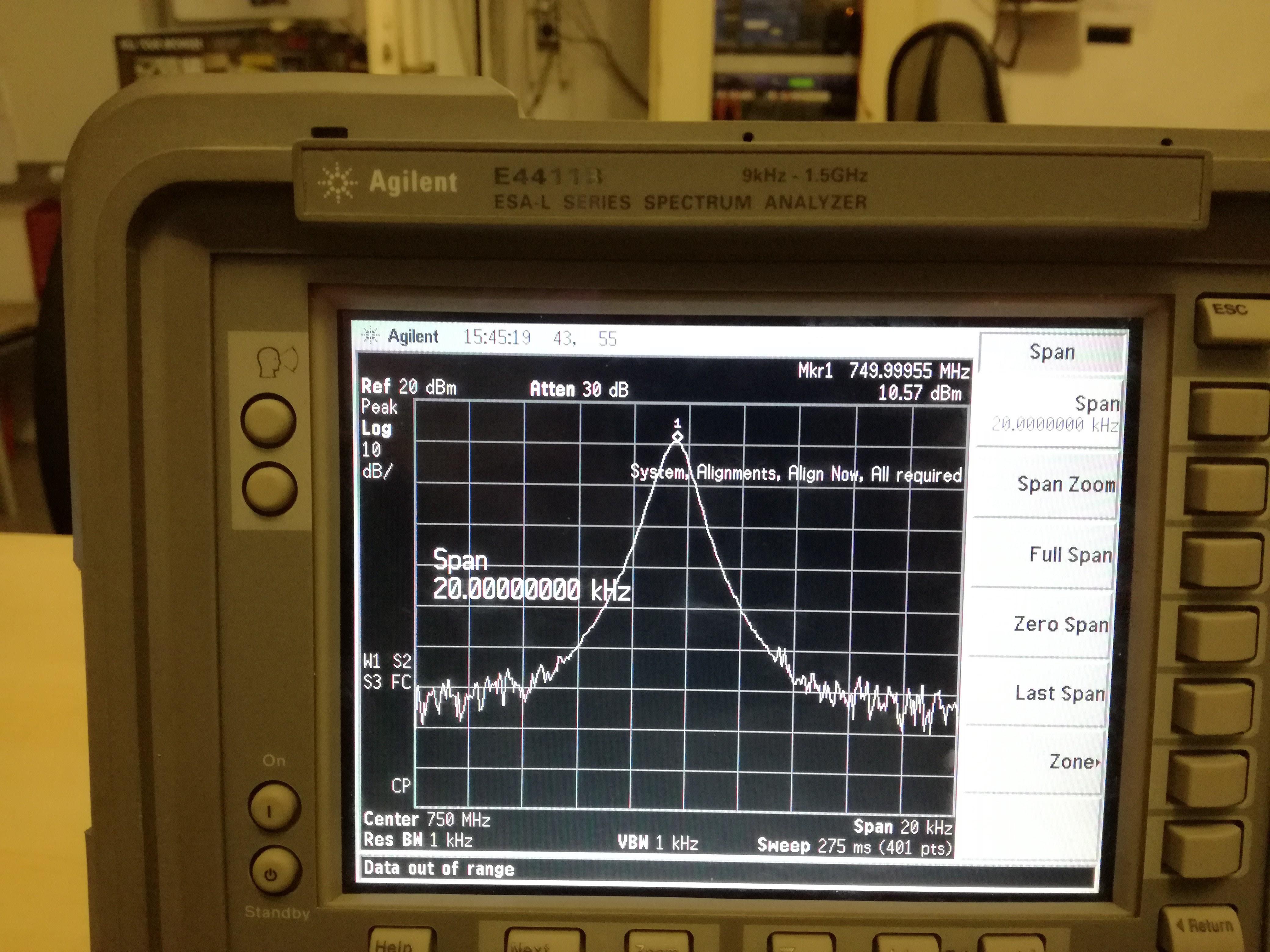
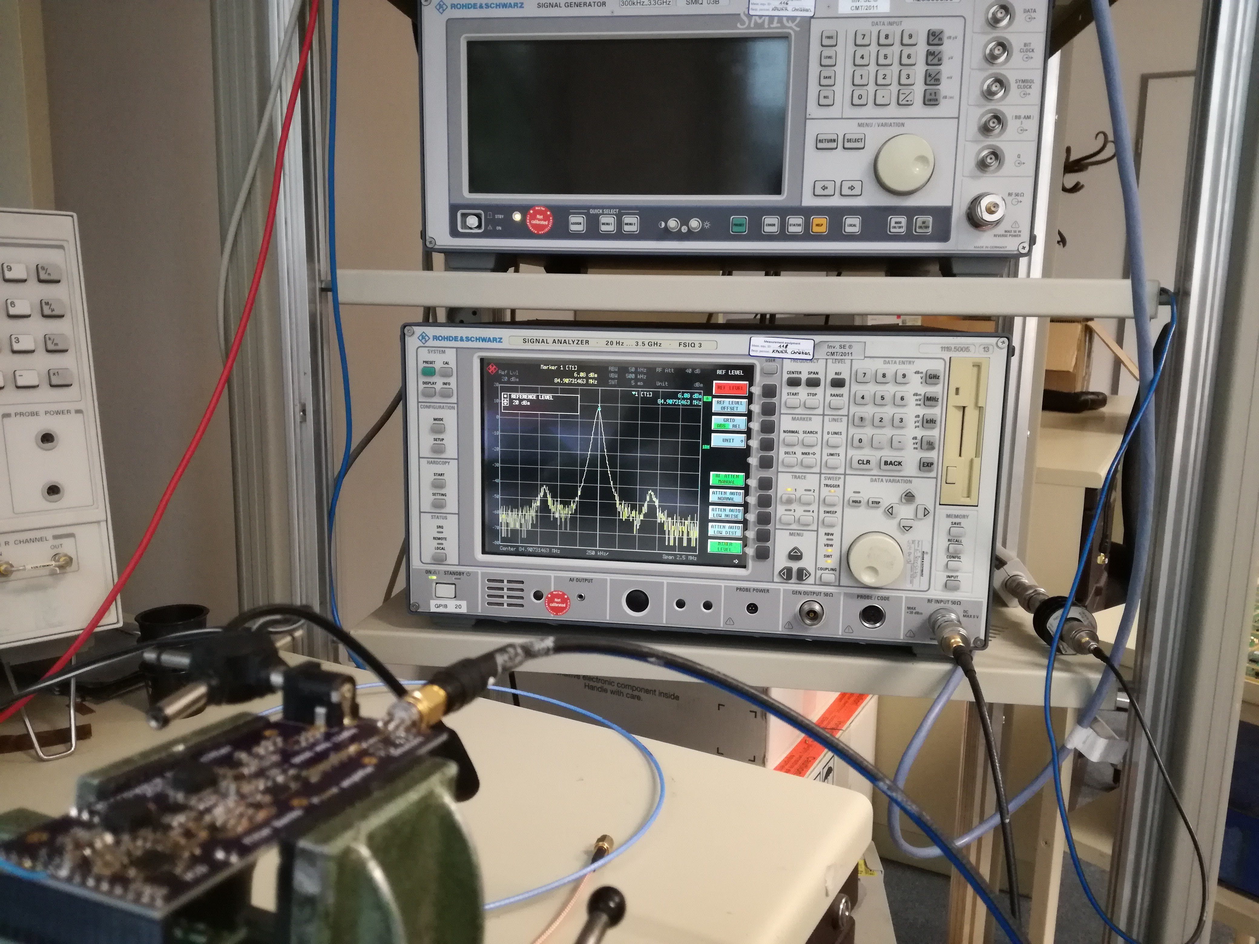
Now that everything's finally working, I could go on and get some real job done here. For instance, to check out what's worth this little MAX2871 chip. What's the spectral content of the synthesized signal? Is it stable? How much does it vary with temperature? What's its quality factor? I used R&S FSIQ3 3.5GHz spectral analyzer to measure all these properties.
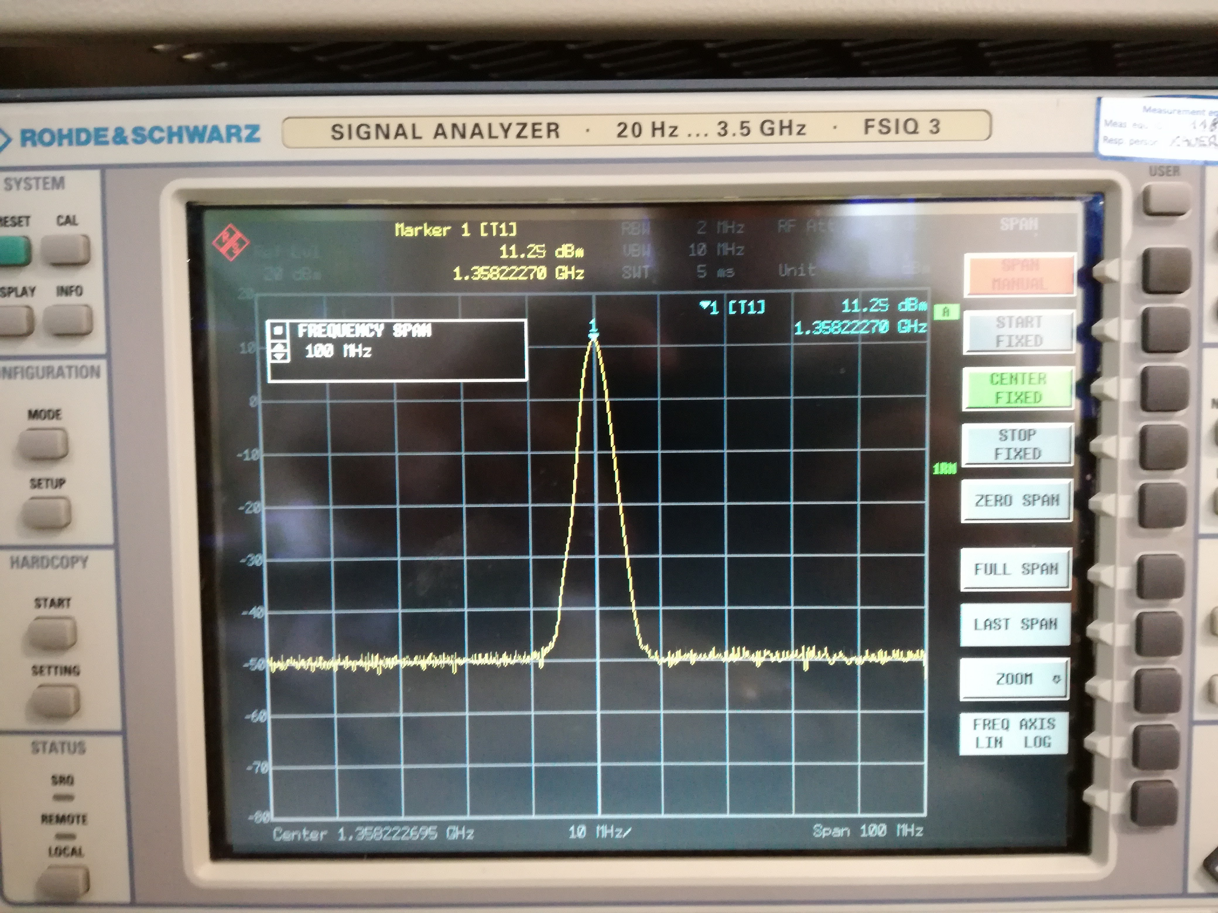
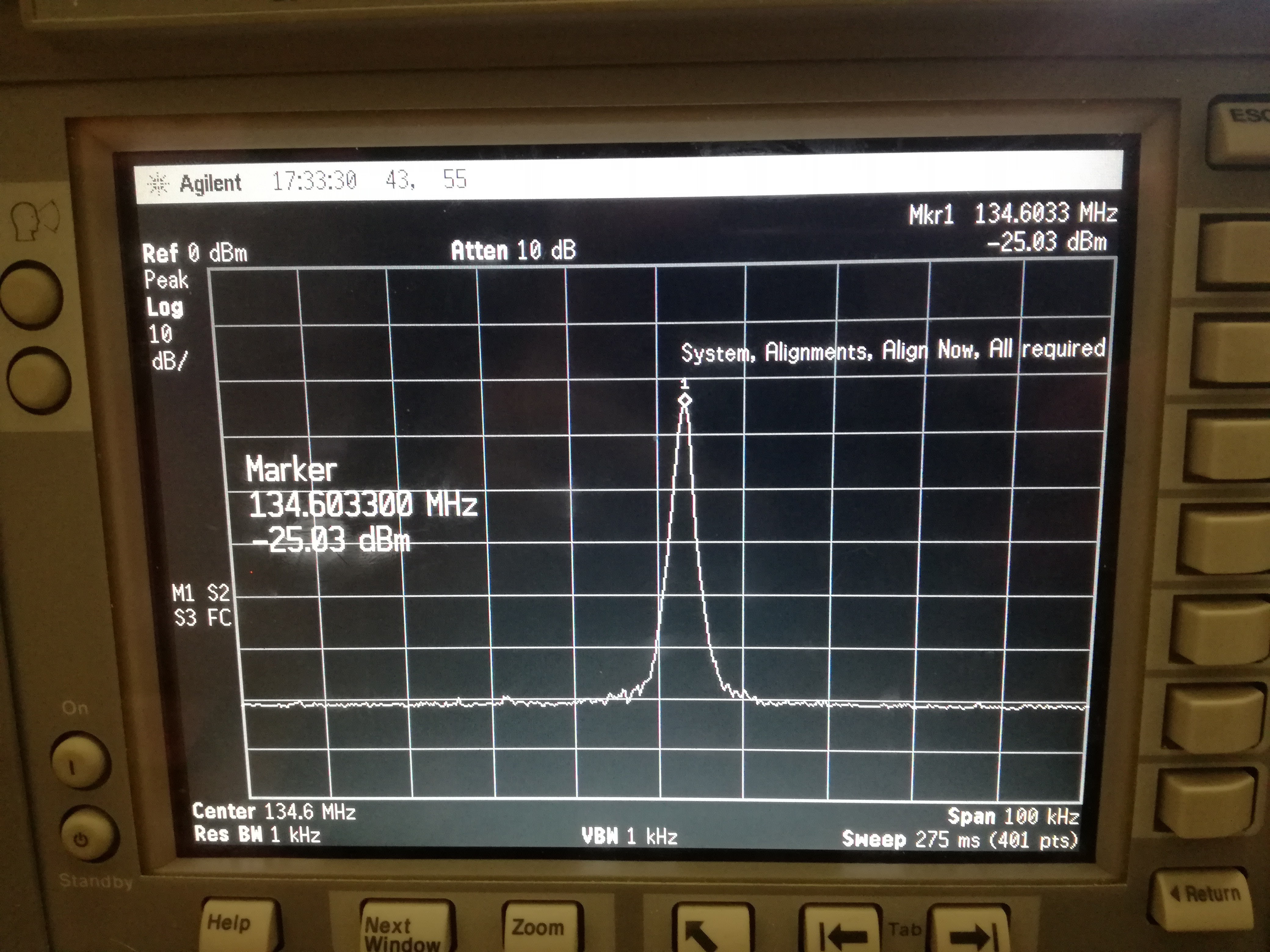
I use my small Arduino program to control the synthesizer ("Basic" example in my Github repo). I can enable/disable RF ports and control the RF output power. Once the transmitter is powered on, I use large frequency span (100 MHz) of the SA to locate the signal. I chose 2 MHz resolution bandwidth to start with. Here we can see nice 11.25 dBm peak at 1.35 GHz (DIVA = 1):
When I reduce the span to 50 MHz, or zoom-in, to be more technical, I observe some funny things (again technical) on the sides of the peak:
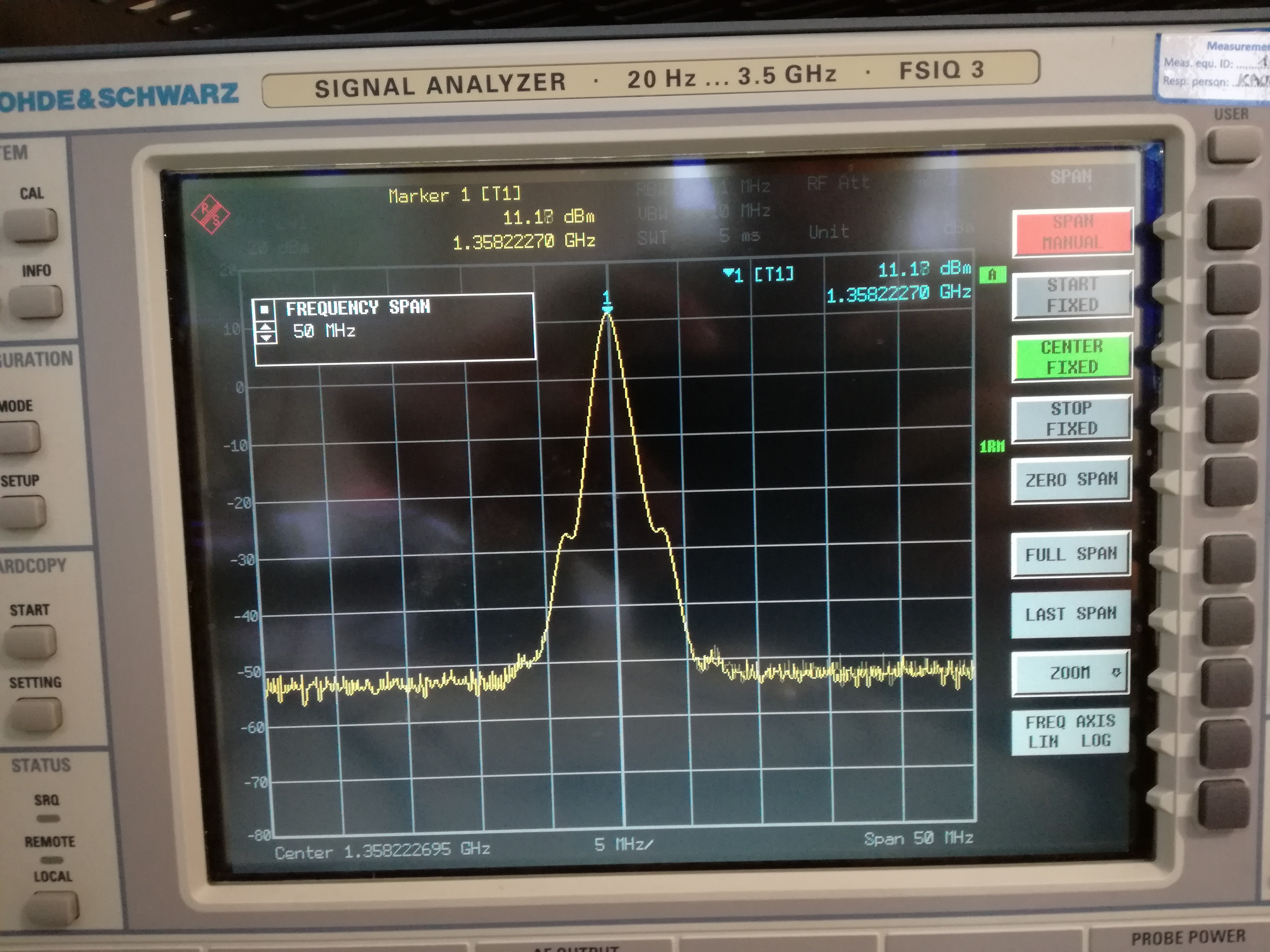
It looks like two small tumors growing on our signal. Further zooming in, we'll see the tumors are becoming real devil's horns:
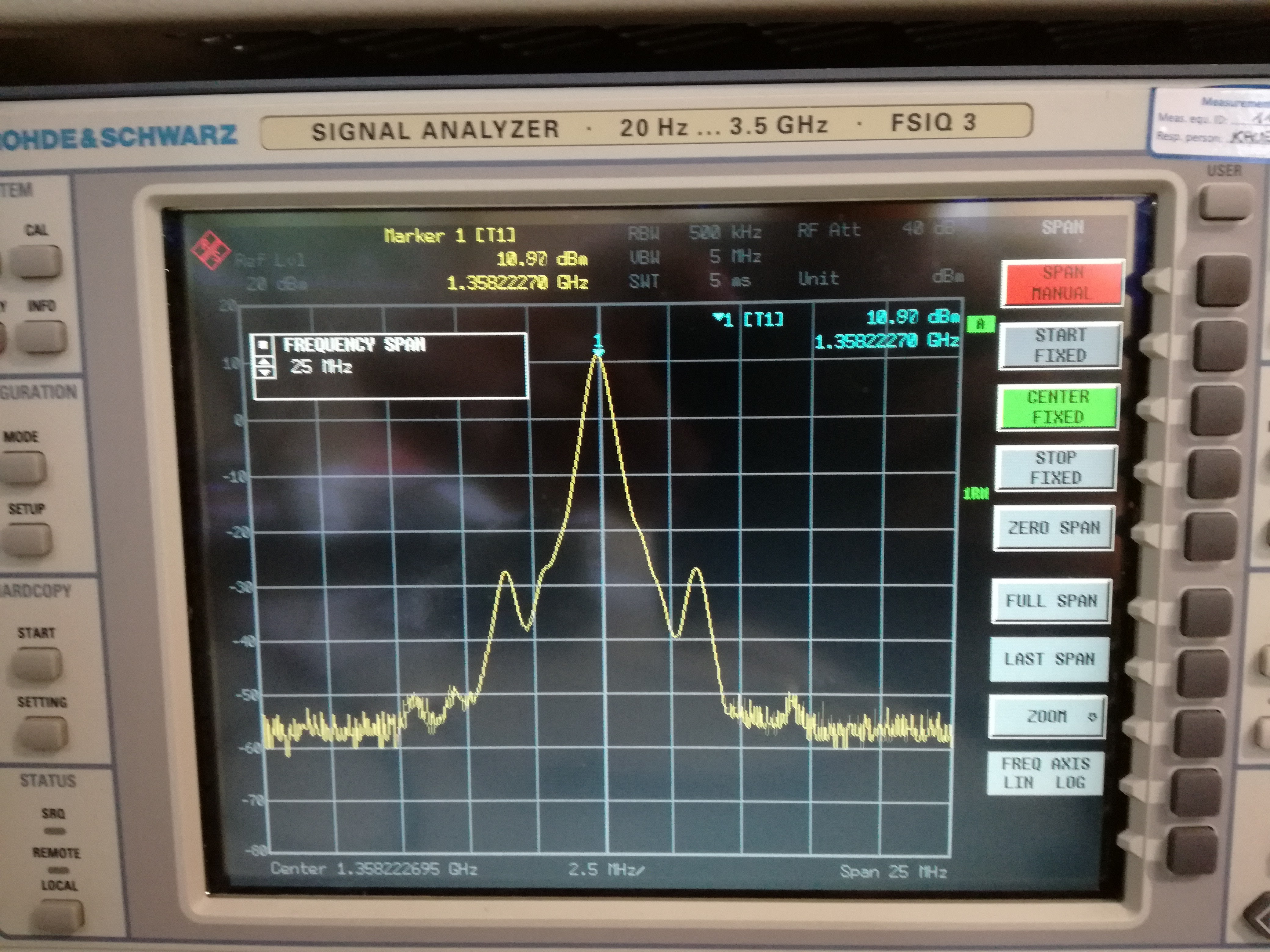
With my frequency span lowered to 12.5MHz, I could see even more peaks unveiling in the spectrum:
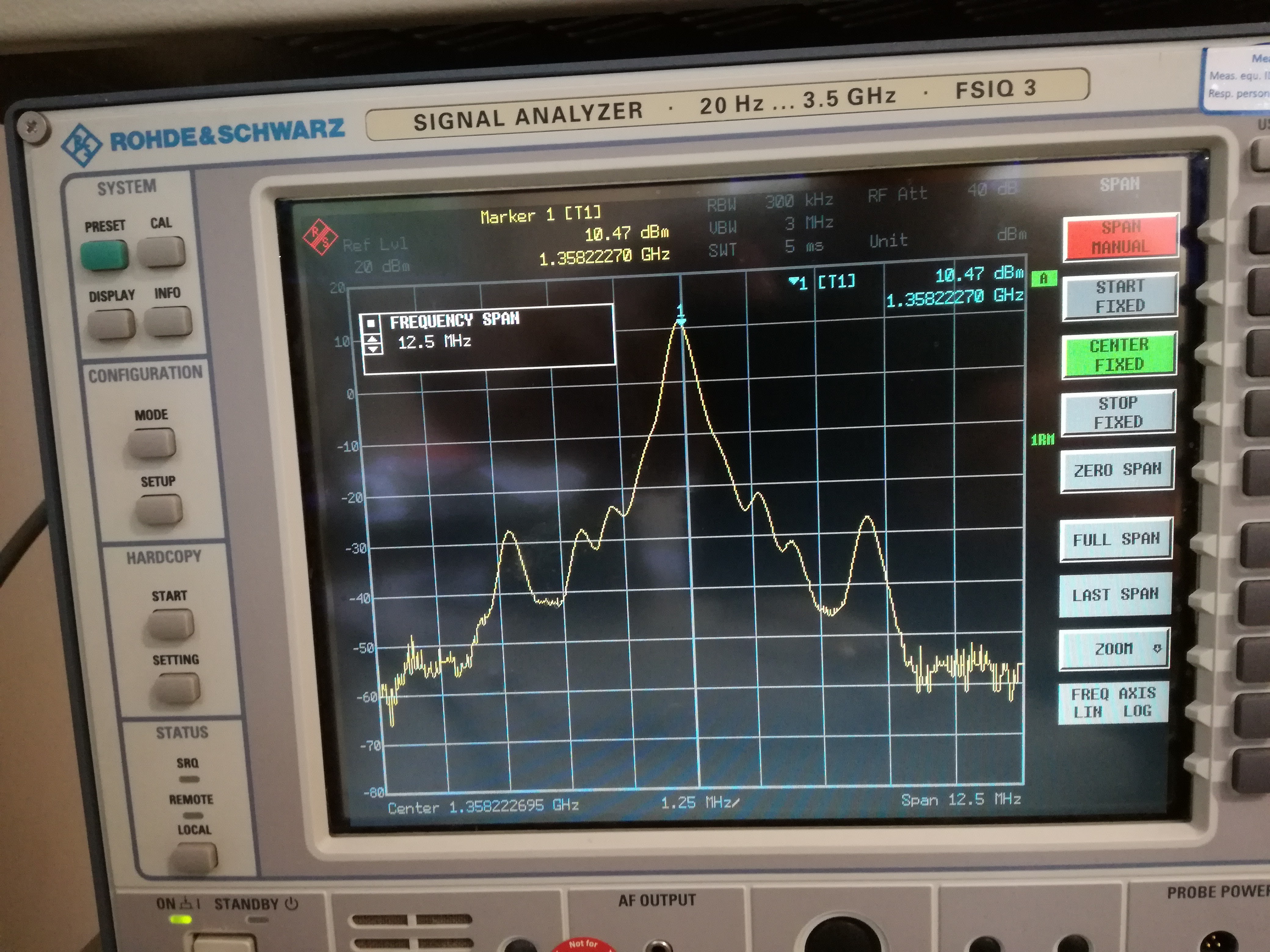
Finally, with span of 6.25MHz, the crystal clear peak turns to be a total spectral jungle filled with side lobes, and multiple order harmonics of some basic frequency transposed to 1.35 gig:
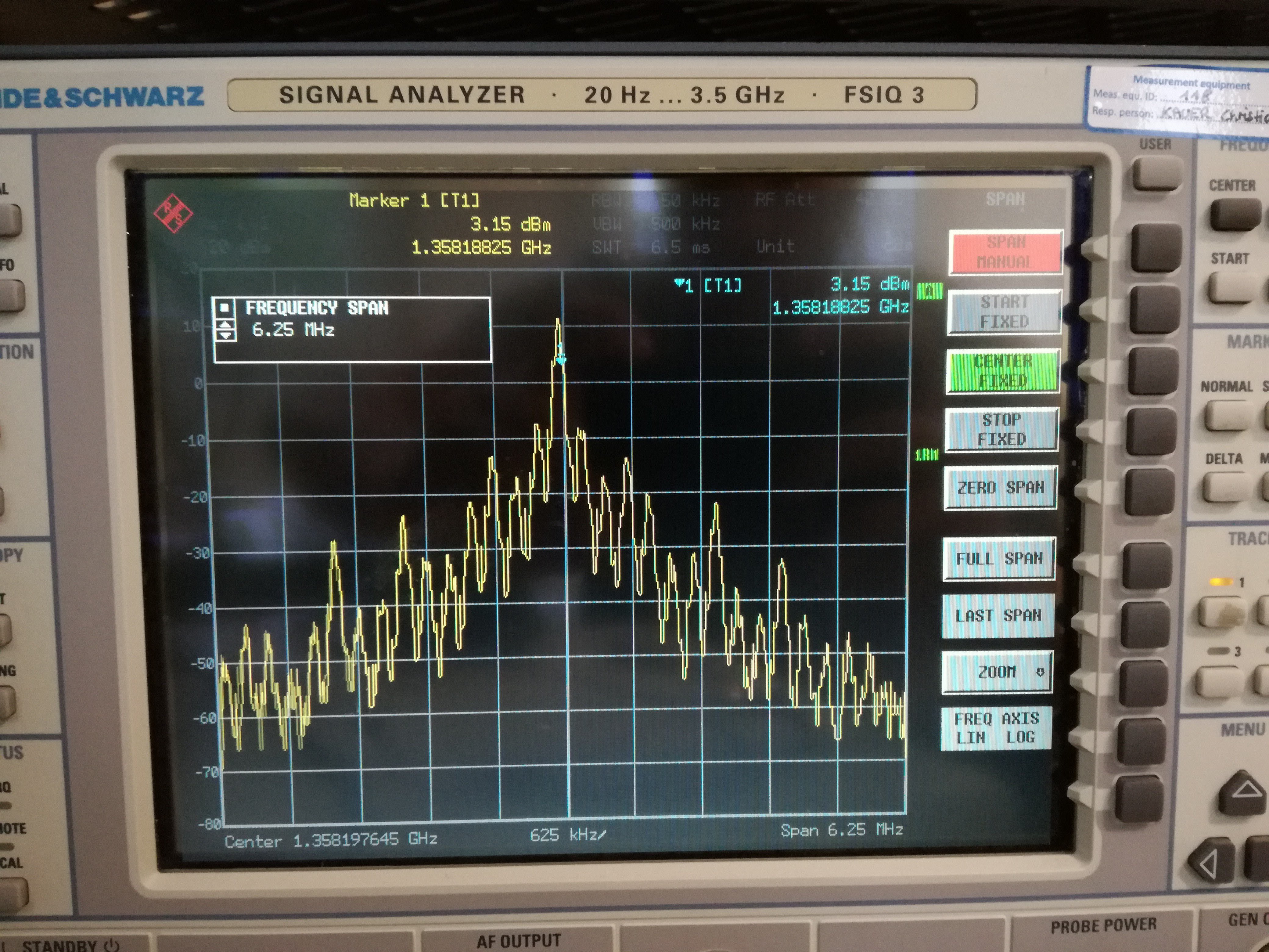
I was expecting that Δf will be around 19.2MHz, what corresponds to the reference frequency of my crystal oscillator. It turned out to be false - the peaks are showing up at irregular distance, hundreds of kHz apart. I can only assume it's some PLL black magic of the MAX chip behind this, like intermodulation products in the chip. Maybe I should start sounding like a professional and address this phenomenon by its name: phase noise. Datasheet specifies it to be -136 dBc/Hz at 1 MHz offset. Since I have division factor N = 135 in the PLL feedback, I can expect additional 20log(135) = 42 dB to the phase noise. It still seams to be much less than what I'm measuring. Could it be chip itself or one more downside of my board (loop filter)?
During these measurements, the frequency drift was barely observable and mostly due to the heating of the chip. I deduct it, as the center frequency only changes when I cool the chip with the tip my finger.
Overall, the synthesizer chip performs well in the frame of what home made, 1st attempt, hobbyist board can hope for. Question that bothers me still is: why is the phase noise so big? why is the spectral content so weird and full of garbage? Why not clean and pointy spike, like I would expect for? Is it caused by the chip itself or by loop filter my board? Is it fabrication trade off for such a wide bandwidth? Questions, questions...I'll start by asking people who made the chip, at Maxim Integrated.
Note on the output power
MAX2871 is said to deliver max 5dBm of power at its outputs. I measure some 11 dBm at the end of my transmitter. Power amplifier TRF37A75 has gain of 12 dB, but programmable attenuator, filters and switches should be 0 dB. In real world that's not the case, so if we're generous, we can say each of them damps 0.5 dB. Together, expected attenuation is (filter, 2x switch, attenuator) some 2 dB. I would add 1 dB for bad soldering on each component (including PA). In total, 5 - 2 + 12 - 5 = 10 dBm, what kinda makes sense with my measurements.
I just want to add that RF power control of the chip worked fine - it really does reduce the chip power in steps of 3 dB.
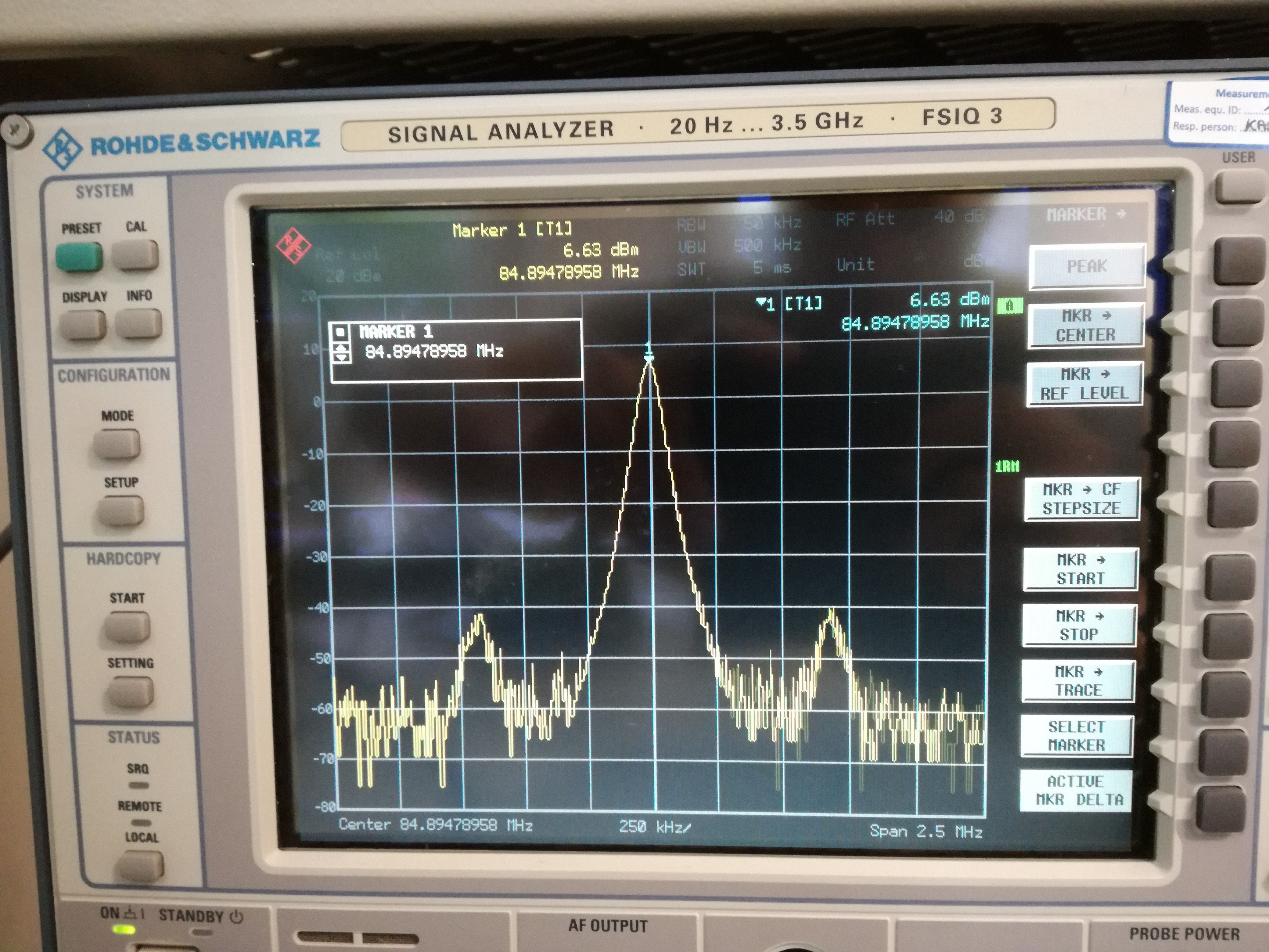
And lastly, I did some measurements at lower frequencies (85 MHz). Total output power in that range was about 6.6 dBm. Hmm, that's weird, all of the components claim to be broadband compatible and I don't expect much loss at such low frequency. Again matter of chip?
Note on the main VCO frequency
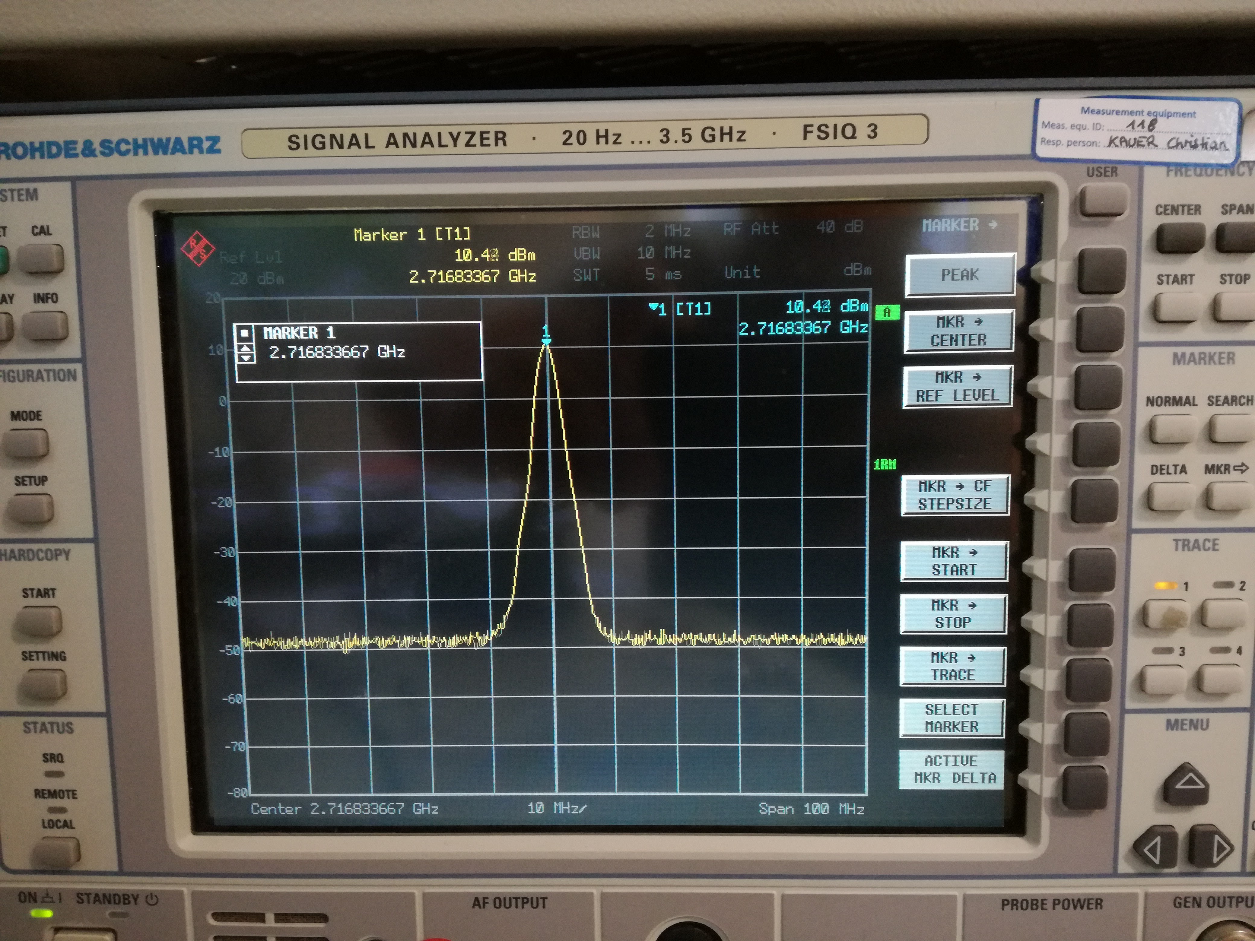
I also wanted to see the max frequency the synthesizer can give (it claims to be 3GHz), so I set DIVA to 0 and powered it on. I measured clean 2.7GHz. Hmm.. where's my 300MHz gone? Bad loop filter? Lying chip?
Note on harmonics
Yes, there...
Read more »I ve finally reworked power amp and tested my board directly over coax cable at the output. It was nice to see that little guy finally works HW bug free.
Here you can see my setup verified with R&S spectrum analyzer.
It's kinda shame to be RF engineer and not own a decent spectrum analyzer... Well, it's on my Christmas wishlist since I was 10, but noone bothered to buy me one so far. RTL-SDR was interesting tryout, but definitely not satisfying enough. Luckily, my local hackerspace has a nice little Agilent E4411B, 9kHz-1.5GHz spectrum analyzer, so I decided to give it a try.
I wanted to see how the signal looks like after every block of the cascade. That's why I used a standard oscilloscope probe instead of SMA cable. Of course, it's a very unprofessional approach in RF engineering, but I needed quick-and-dirty way to investigate my board. Hopefully, if I reduce the frequency low enough, the RF black magic will spare me some meaningful insight.
And here's the spectrum of my signal, directly at the MAX2871 output. It doesn't look bad at all! It's very narrow banded and stable over the time. It's only weakness is that it's..er..weak. It peaks to -25 dBm, while the datasheet specifies it should be minimum -5 dBm. What could make it this small? Bad soldering? Some capacitive leakage that I'm not aware of?
The following table shows the signal power after each element in the circuit:
| MAX2871 | -25 dBm |
| 1st switch | -29 dBm |
| 2nd switch | -32 dBm |
| PE43711 (set to 0 dB att) | -32 dBm |
| Power amp | -43 dBm |
| Coupler and connector | -43 dBm |
And we have a winner! The biggest damper is, ironically, power amplifier. I assume it's only one more bad soldering job, as many others on board.
So, the next task is, obviously, to rework the power amp. And for the future testing, stay out of RTL-SDR based spectrum analyzers.
Verifying that all components are working properly enables me to run the first functional test of the MW transmitter - frequency synthesis. In the repo, there is "Basic" example that configures MAX2871, attenuation, filter and ADC for RSSI detectors (even though the latter ones do not work, presumably).
The configuration is set as follows:
I intentionally set the DIVA so high so that I can measure the output frequency with my RTL-SDR dongle. With 5 dBm there should be no problem detecting some signal.
The "Basic" example makes user choose register content readout and turning on/off the RFOUT.
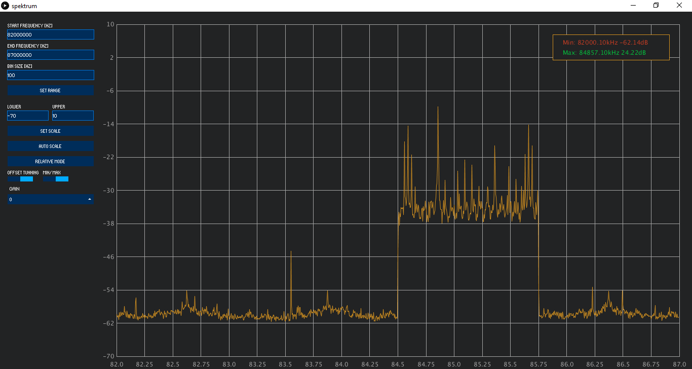
However, things didn't go as planed. Good things first: there was some output, and I could control it (turn it on/off) with my program. Bad things: The signal was very low, way below the expected 5dBm level. And it was also very wideband and filled with spurious content. Here's an example screenshot from RTL-SDR that runs "spectrum analyzer" program.
I cannot say that the basic functionality test has been passed, so the further investigations and debugging must take place. I'm just not sure where to start looking from. Is the MAX chip configured poorly (it shouldn't be, I used configuration from datasheet example) or do I get some terrible damping from my circuit?
After verifying the main chip, MAX2871, it would be nice to see if other components work as well.
First, I tested 4PST switch SKY13322-375LF. The switch is controlled with 4 parallel inputs that switch RF input to one of four outputs. I wrote a simple code that allows user to chose (and change) desired output and measured the connection between input and corresponding output. I was hoping to hear that lovely "beep" when I send certain character on the serial terminal. Guess what, it didn't work. There was short circuit to the GND from all outputs. Bad soldering job with my reflow oven. After the rework, everything worked fine.
Second thing was the attenuation chip PE43711. It is controlled over SPI and attenuation can be set in steps of 0.25 dB with more or less precision over the frequency range. The attenuation is calculated as an 8-bit word/4. Since the chip doesn't provide any data output, I only could test it with a multimeter. I measured input and output resistance as well as resistance from input to output with various settings. My observations are in the table below:
| Attenuation, dB | R in | R out | R 1-2 |
| 0 | 42.7k | 42.7k | 11.6 |
| 1 | 381 | 369 | 16.7 |
| 2 | 195 | 175 | 21 |
| 2.25 | 175 | 155 | 22 |
| 3 | 138 | 119 | 25 |
| 6 | 81 | 62 | 38 |
| 10 | 63 | 45 | 52 |
| 20 | 52 | 36 | 73 |
So, the resistance changes when different setting is chosen. I guess this suggests that SPI and chip work.
Power amplifier doesn't provide any meaningful testing options - I can only hope it works when it is powered on.
RSSI detectors are weird. I can measure detected signal using the ADC on Teensy. However, measured voltage is somewhere around 0.3 - 0.5V, even though there is signal at the input. Interestingly, the measured value drops to 0 when I put the voltmeter on the output pins. I have no explanation at the moment. My only guess is that troublesome soldering of BGA chips resulted in bad joints and ADC input measures any picked up voltage. Voltmeter probably than acts as a pull-down resistor and sets the measured value to 0.
Overall, since synthesizer, switches, filters, attenuation and power amp work, I can hope to see generated signal with a spectrum analyzer. When I get one.
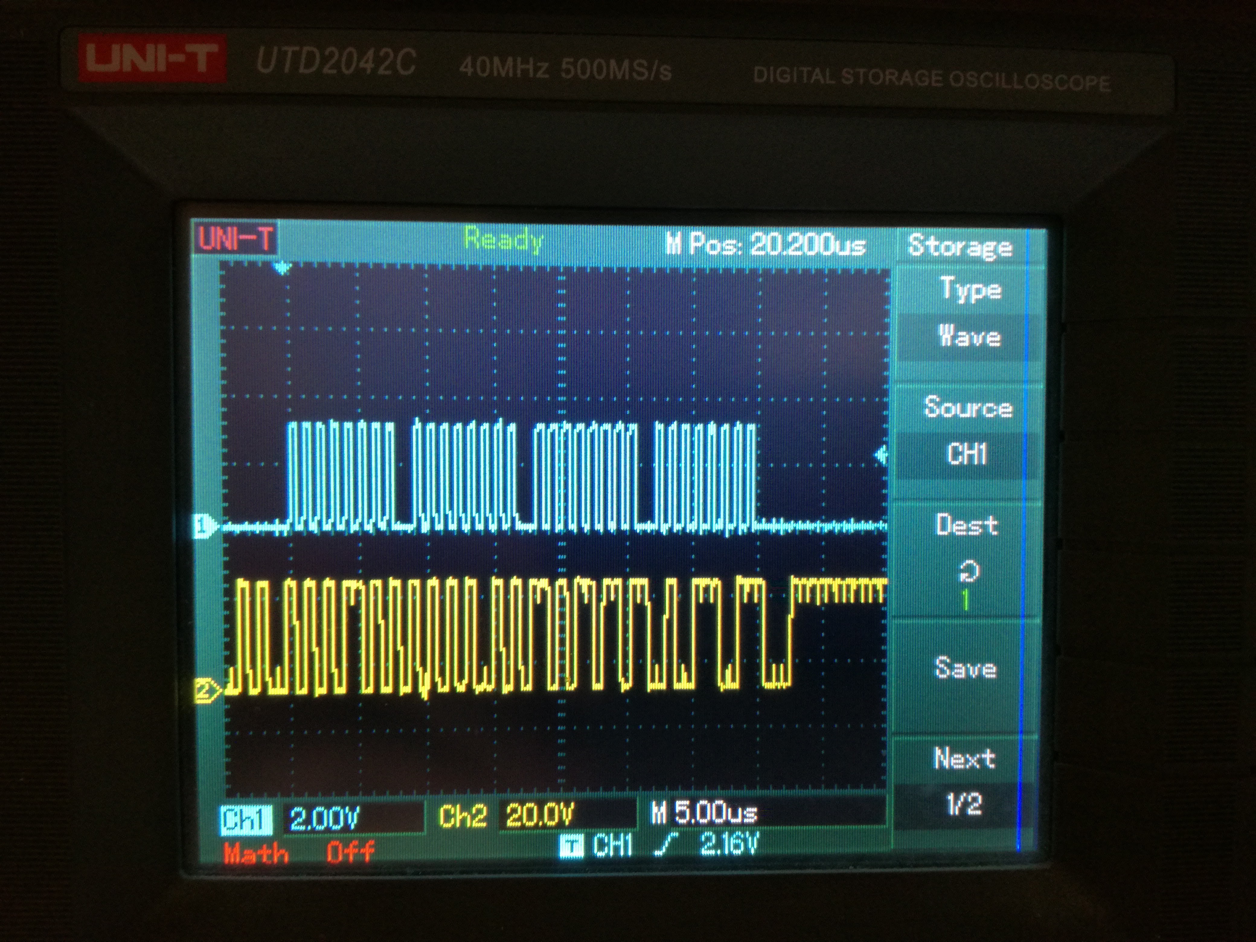
It really took a long time to get the damn MAX chip working. Although I made it set MUX line high or low, I couldn't make it talk to me via SPI. On the scope, this line looked like nonsense:
In the process of investigating, I managed to burn 3 Teensy boards and 2 MAX chips. Don't ask how. I consulted tech support of Maxim Integrated as well. They were really friendly and prompt reacting (thanks Mohammed). But, before I got the answer from them, I decided to try one thing.
MUX bits are distributed in two registers. MUX[3] is in reg 5 while MUX[2:0] in reg 2. My initial code was writing reg2 first and reg5 later. For no clever reason, I decided to switch the order of writing. Guess what? Problem solved.

Aaaargh!
Synthesizer MAX2871 can be configured using SPI on one of its six 32-bit registers. To test if everything works fine, I wrote a prompt Arduino program that runs the SPI bus and configures these registers in very simple way: setting pin MUX of the MAX2871 high or low. This is done by setting adequate bits of registers 0x5 and 0x2. this pin can also be configures as SPI data out (MISO) pin that reads out the contend of the only read register, 0x6. The read data is chip ID, ADC code and VCO status.
The program initializes the chip (programing all registers twice) and toggles MUX pin high and low every two seconds. After user input on serial port, the program displays read data from the above mentioned register. However, while the pin toggles fine, what led me to believe that SPI works as it should, read out makes troubles. It reads code that makes no sense. Still to be checked.
Read more »


I've just completely re-read your project and it's inspired me to build my own RF signal generator to test my own 4G repeater with. I'm going to use the ADF4351 + LCD keypad shield + some resisters + Arduino Uno as documented here: http://f6kbf.free.fr/html/ADF4351%20and%20Arduino_Fr_Gb.htm
... And hope to save myself $600 on buying a second hand signal generator for up to 1000 MHz.

Hey, cool project! I've had similar trouble while using RTL-SDR as a spectrum analyser, so I'm glad I'm not the only one :)
I wonder why the RTL-SDR failed? I've also got the LimeSDR so maybe that will work better with this type of signal generator?
This looks like a very interesting project for me. I'm wondering why you've not got an LNA (low noise amplifier) in the circuit?
I'm using this one myself, but it only goes up to 3.8GHz:
Mouser Part No: 772-QPL9065SR
Manufacturer Part No:
QPL9065SR
Manufacturer:
Qorvo Qorvo
Description:
RF Amplifier .45-3.8GHz NF .55dB Gain 37.5dB
I was thinking of placing an LNA on the detector side, but seeing that detectors are good enough to detect really low power levels on their own, I said, nah, don't wanna bother with additional components. It's already anoying enough for manual soldering :)
Great! Hey, I don't suppose you could have a quick look at my repeater project:
https://hackaday.io/project/20500-cell-phone-signal-repeater-booster-femtocell
any comments / feedback would be useful. I'm kind of struggling with it at the moment. Thanks!
I did take a look at your project, and boy does it seem cool! Great job, man! Keep up the good work. I however, have not much to say about it, since I have no experience with LimeSDR nor did I ever do anything with GSM/LTE systems... I could only drop by if you have some HW design problems to look after.
Actually the project is comprised of two parallel solutions - one using the LimeSDR and the other using hardware only. The LimeSDR is fairly difficult to set up although I have had some help from the engineers that built it, by bribing them with homemade hot chilli sauce!
The hardware solution is being done in 'simple' blocks, each one on it's own PCB and connected by U.FL cables. Currently I have blocks for duplex (bandpass) filters, low noise amps, variable gain amps, fixed gain amps and am using the LimeSDR as a spectrum analyser. I'm not trying to process the signal in any way at the moment - just filter it and amplify it. It should be simple if I really knew what I was doing! Some of the blocks are working and others are not and there are a couple more to assemble when I have time.
Please feel free to join the project :) HW input would be really useful.


 Yann Guidon / YGDES
 Nick Sayer
 Emilio P.G. Ficara
Is this a copy of the Single MW source from J.Hermann or the other way around?
http://microwave-jh.com/single_source.html