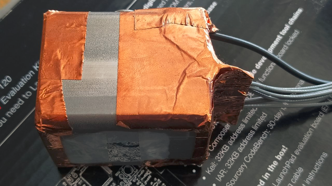
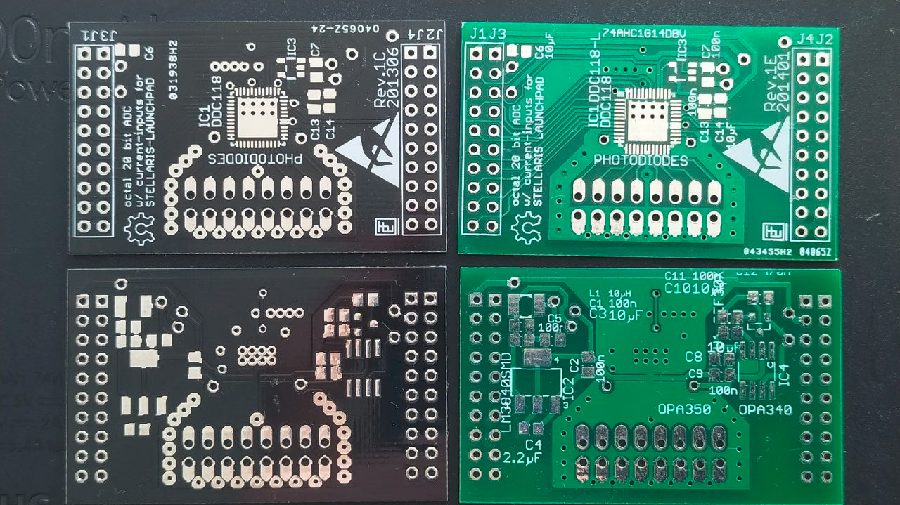
• Perovskites

    helge06/03/2023 at 07:31 0 comments

    A news flash on Hackaday (1) highlights recent work (2) on using Perovskite pixel mosaics to implement multispectral imaging. Similar to Sigma Foveon sensors, layers can be stacked in the optical path to obtain a spectral decomposition of the incident light rays.

    The reconstruction is achieved through fitting of a set of coefficients which approximatively encode the inverse transform to the spectral cross-talk owed to overlapping absorbance spectra and incomplete extinction (= "neuromorphic" in fancy-speak).

    Depending on the chemical composition, different absorption edges are found:


    Unlike the Foveon sensor though, at this stage, the authors do stack this sensor together with individually spin-coated, laser machined and pre-qualified single-Perovskite sensor planes:

    "Figure S28 displays the testing setup, where we used a projector (M6 Pico Projector, AAXA Technologies) to generate a panchromatic source image and used a lens to focus the incident light onto the chips. Blue, green, and red chips are sequentially stacked (six-terminal stacking) from front to back, where blue, green, and red channels of current are read out independently."

    Which is fine for the paper, but points at the compounding difficulty of 2.5D integration - a factor which translates into years of research and a super-linearly growing difficulty in adding more and more spectral bands.


    Perovskites are envisioned to be put on plastic foils (3) for solar photovoltaics applications, but here sensors can be kept under vacuum or inert gas in hermetically sealed ceramic packages with glass windows, eliminating some of the stability issues with this class of materials (4):

    But if I were to bet, I think it's more likely we'll see Bayer pattern and, at best, 4-6 wavelength sensors with more elaborate CFA-like patterns (5) before high integration happens:

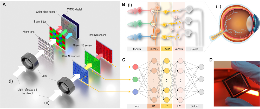
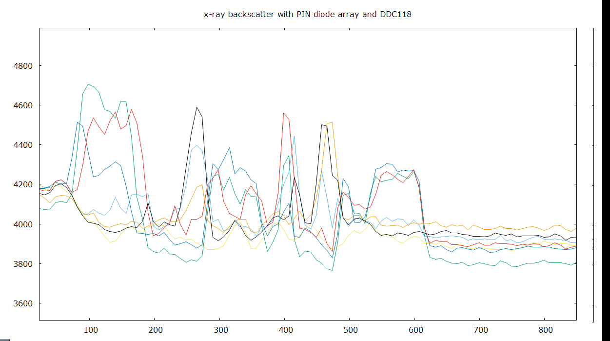
    For the proclaimed satellite imaging applications (if lifetime issues can be controlled), sequential stripes in push broom imagers should rule out the need for intricate, low-yield stacked pixels.


    Addendum: just how hard can it be? "Non-dissipative internal optical filtering with solution-grown perovskite single crystals for full-colour imaging" (7) has you covered:

    and in "Beyond Tristimulus Color Vision with Perovskite-basedMultispectral Sensors" (8):

    (Note: the C1-C2, C3-C4 and C5-C6 stacked perovskite layers should be similar to gradient engineered light absorption layers, not anti-series diodes. The illustration is a bit strange in that regard. Figures S14 and S15 show adequately contacted organic diode structures as well.)

    "Direct contact of perovskite layers appears challenging in the view of known halide-ion mixing. This problem might be mitigated by insertion electrically conductive, optical transparent and halide-ion-impermeable contact layers."

    Essentially, some form of mesa etching, passivation, barrier contact formation and metalization would need to take place, as sketched below:

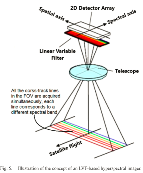
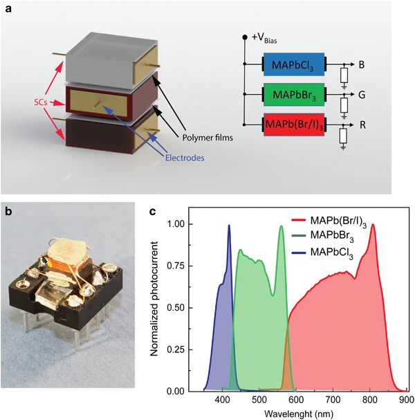
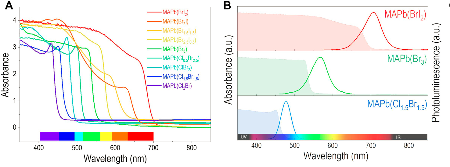
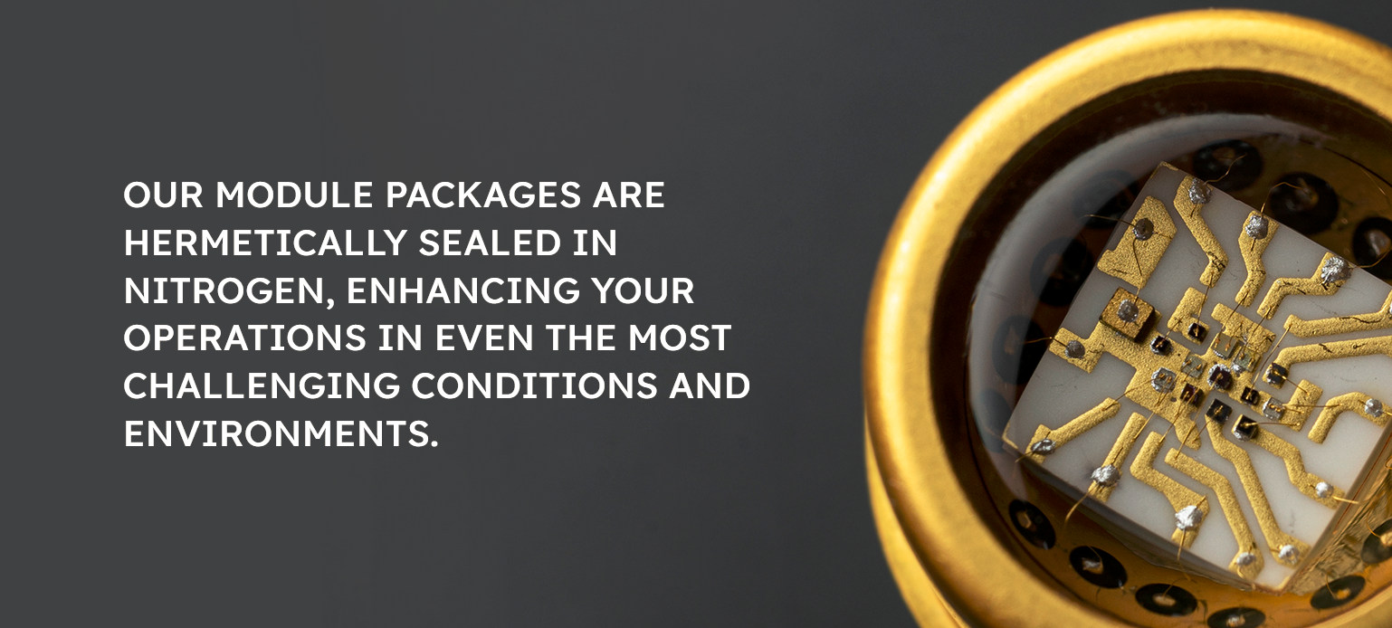
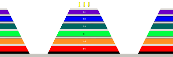
    This looks a lot more involved than the initially advertised simple spin coating process and resemble what is being done to form III-V diode structures (9) and lasers.
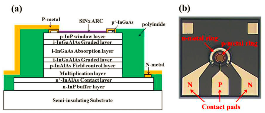

    References

    1. https://hackaday.com/2023/06/02/perovskite-sensor-array-emulates-human-retina-for-panchromatic-imaging/
    2. https://www.science.org/doi/10.1126/sciadv.ade2338
    3. https://onlinelibrary.wiley.com/doi/full/10.1002/adem.201901217
    4. https://www.frontiersin.org/articles/10.3389/felec.2021.712785/full
    5. http://www.quadibloc.com/other/cfaint.htm
    6. https://doi.org/10.1109/JSTARS.2021.3090256
    7. https://www.nature.com/articles/am2017163
    8. https://pubs.acs.org/doi/10.1021/acsami.1c25095
    9. https://doi.org/10.3390/s19153399

  • A Few Pictures

    helge03/25/2023 at 13:28 0 comments

    1 Signal GND shield over IC and input-side pads.

    of 2 u.fl connectors added instead of 2.54mm pin headers.

    3 pin diode array with Pb aperture. Signal GND inside is left disconnected from the sensor head chassis GND and only connected on the DDC118 board.

    4 An incomplete iteration - the LDO is still on Rev.1E. Attempts were made :)Should I have a need to build another board, it'll probably look very different today.

    • u.fl connectors are okay for prototyping and even for photo diodes spread across a larger area, but it serves well to keep everything on the same PCB. Whether it's worth moving to shielded mezzanine connectors or not, remains to be seen.
    • Common-mode noise isolation via digital isolators.
    • separate board with JST XH or Molex KK 254 header..
    • Common-mode filter in the power supply lines. Local 5.0V LDO. Optionally a low-noise isolated converter can be used (Ti SN650x + transformer).
    • An array of DIP switches to short every input individually. Alternatively, the board could also be fitted with a flexprint connector to minimize the length of input traces / exposed conductor length. A folded piece of Cu tape, or a bit of Nickel foil can be inserted into the FFC header.
      These ICs are highly susceptible to ESD damage, and separate protection diodes might invite unwanted leakage paths. For assembly, transportation and initial tests, all inputs should be connected to signal GND. DDC118 is rather expensive, so it's hard to imagine scenarios where it should be exposed to damage.
    • Source-side series termination resistors in the data lines could reduce any possible impacts of fast slopes.

    WE-SHC shielding components:

    WE-SHC Shielding Cabinet | Passive Components | Würth Elektronik Product Catalog

    Hirose DF40GL shielded mezzanine connectors:

  • Ushio Epitex to deliver 8-LED clusters

    helge12/14/2021 at 12:15 0 comments

    A recent HaD article highlighted an LED array reflectance sensor for plastics identification. As it's obviously related to this project, I've rummaged around for another source of LED arrays for hyperspectral imaging, absorption / reflection spectrometry and spectral fingerprinting. Check out USHIO's 8-in-1 LED package with a miniature BGA footprint.

    It's really becoming clear how these emitters could pave the way for hyperspectral imaging integrated into smartphones, as they are a lot better integrated than single LEDs. Smartphones might even be reworked to replace the LED light / flash with a multi-spectral source for such occasions.


    I can also see how a repeating pattern of sequential light pulses can be combined with short exposure times and a rolling shutter sensor to extract a lower-resolution 2D hyperspectral image. Shout-out to [Jerry de Vos], [Armin Straller], and [Jure Vidmar] :)


    https://www.ushio.eu/multi-wavelength-leds/

  • "Infrared-based sensor system for contactless monitoring of wetness and ice"

    helge07/05/2021 at 15:53 0 comments

    Here's an inverse solution - when detecting in a wavelength range where LEDs are the go-to light sources and consequently narrow-band, multispectral sensing is easier to do, and the spectral resolution is more sharply defined.

    This goes both ways though, as a set of LED dies needs to be available for both photodiode-mode and emitting diodes.


    https://jsss.copernicus.org/articles/9/133/2020/

  • Senop makes them!

    helge03/01/2021 at 16:22 0 comments

    Sometimes I find I entertaining how ideas go full circle. As I was researching some other optical principle, these "multichannel optodetectors" crossed my way. They're effectively what I was striving for with the Optical inch project, albeit at a more reasonable price point than these hermetically sealed optical hybrid modules ;)


    Meanwhile I'll keep claiming the approach with LEDs while it lasts.

    https://senop.fi/industry-research/electro-optical-components/?gclid=Cj0KCQiAvvKBBhCXARIsACTePW_9TKZ8SHfsQSvjR5_61XxJX4urAwqVYn11wzNPV1-3hjlV2FYxYHYaAo65EALw_wcB


  • achievement unlocked: x-ray vision

    helge04/10/2017 at 20:59 0 comments

    40x40 mm² stainess square tubing with 8mm tapped holes - one for mounting an aluminium cube, the other to pass the "light" through and the PIN diode array PCB glued to the cube. Add a 1.5x3 mm² pinhole made from 2mm thick lead sheet, light seal all openings with copper tape, Al tape over the pinhole. Done. Note: this is not a transmission measurement but a backscattering geometry.

    horziontal: time (50ms intervals), vertical: 7 of 8 channels (something went wrong, maybe a connector came off...)

    What you see here is the raw 1D image of an 8 pixel x-ray pinhole camera observing a piece of stainless steel illuminated by an x-ray tube ~8cm away as I'm waving it around (duct-taped to a PP tube and held where the dose rate is <2µSv/h).

    ...And here's just the channels with a bit of smooth kdensity. At approx. sample #610 the x-ray supply is switched off.

    It has proven effective to let the analog ground float inside the metal enclosure and connect case GND to the digital ground of the launchpad.

    Let me conclude this log entry with a snapshot of the pinhole camera setup. Note this is a different board but I still put that Faraday shield over the exposed input pads. Black cable is chassis GND.

    edit: Settings: 18kV, 110µA. Nice.

  • overdue layout update

    helge03/27/2017 at 01:26 0 comments

    "I still have the parts for your DDC118 booster pack, do you have any assembly instructions?"

    "throw that old PCB away"

    Here's the new one. Guess I'll find out tomorrow that those u.fl connectors are spaced too closely or that the diff pairs have a polarity twist somewhere.

    new minor revision:

    - has proper footprints for U.FL connectors. They feel right for the job, right now I don't care much about the added capacitance due to coaxial cable

    - tidies up passives

    - actually spells out the channel numbers at the connectors and signal names near the pin headers ;-)

    - removes LDO

    - introduces differential DIN / DOUT

    - introduces series termination resistors

    - has 2x1 receptacle and 2x2 pin header for stacked daisychaining (first board has GND jumpers, all except for the base board omit R5/R6 in favor of a pair of wires that re-route DOUT/!DOUT, last board is unmodified (not pretty, but I couldn't be bothered to go 4-layer at this point

    - introduces NC7SZ175 SC70-6 single UHS D-type flipflop which synchronizes CONV transitions to CLK_4X rising edge within < 5ns as per requirement (ds: sub-10ns for best performance), since I don't want to ensure these stay synchronized no matter what the Timer/Counter configuration I'll sync it in hardware. Will have to investigate beating anyway (+/- 0.5 clock cycles = 200-250ns w.r.t. 100µs-10ms integration time...)

    - not yet given up on shields

    - short circuits at the corners to avoid power-up when board is in wrong orientation (avoids killing the expensive IC)

    "todo":

    - see if moving SPI clock (not in sync with converter) up past the REF3040 (U1) changed anything

    - not too excited about those digital traces running across the reference buffer. DOUT/!DOUT now diff routed to cancel capacitively coupled possibly async (w.r.t. ADC clock) bitstream, async SPI clock trace relocated, rest of the signals are static

    - build 2 new boards and use a full 16 pixel sensor. Oh boy...

    ____

    edit: had a few hours of sleep, found mistakes and fixed them ;-)

  • SPM64 kills the optical inch (for VIS-IR)

    helge02/16/2017 at 09:41 0 comments

    What's more important - achieving a goal or seeing a project through? You decide. ESPROS obviously managed to get a simple (diffraction based?) filter matrix slapped onto a camera sensor, making a cost effective and elegant device called Viavi.


    Need UV A/B as well? Grab a VEML6075.


    Meanwhile the Optical Inch will continue its journey with an LED array and Si PIN diodes for in-situ x-ray imaging. Stay tuned.

    https://www.espros.com/photonics/spm64/

  • AS7263 - A near miss to the Optical Inch

    helge01/26/2017 at 13:37 2 comments

    Just found this very interesting simple-ish NIR spectroscopic fingerprinting sensor which goes in the general direction of the Optical Inch. Same class of device although the impelementation is quite different because it uses dielectric narrowband filters.

    Time will tell if this will evolve and how filter based arrays compare to the Optical Inch band gap array.

    How do you feel about commercial products that crop up and do similar things to what you're working on?

    _________________________________

    6-Channel Visible Spectral_ID Device with Electronic Shutter and Smart Interface


    "The AS7263 is a digital 6-channel spectrometer for spectral identification in the near IR (NIR) light wavelengths. AS7263 consists of 6 independent optical filters whose spectral response is defined in the NIR wavelengths from approximately 600nm to 870nm with full-width half-max (FWHM) of 20nm.

    An integrated LED driver with programmable current is provided for electronic shutter applications.
    The AS7263 integrates Gaussian filters into standard CMOS silicon via Nano-optic deposited interference filter technology and is packaged an LGA package that provides a built in aperture to control the light entering the sensor array. Control and Spectral data access is implemented through either
    the I²C register set, or with a high level AT Spectral Command set via a serial UART."

    article http://www.azosensors.com/news.aspx?newsID=11749

    distribution http://ams.com/eng/content/download/976611/2309519/498778 (Digi-Key $4.90)


  • exchange recent updates for working board

    helge01/13/2017 at 16:48 1 comment

    In the previous log it was shown that half of the ADC turned out to be non-functional. Luckily it wasn't the last board so another one was grabbed.

    A few hours later we have a modified PCB with 1.27mm headers (perf board circles cut in half to yield 1.27x2.54 grid pads

    and thanks to quick delivery from China also a big pack of u.fl cables and connectors (sculpting the pads-to-be for U.FL was something that made me want to redo the PCB - Rev1E PCB on the right is for reference so you can see the GND polygon)

    Here's the fun part: soldering the U.FL cables and attaching 0.635mm wires to route the connections to the diodes

    and it's done. Let's mount the PIN diode array (it's hard to see but there are 2 diodes on each of the 8 chips, 16 pixels in total, only the upper half is in use right now)

    I haven't bothered to get the pinout right so the channels are out of order but you can convince yourself that

    * all channels are working to spec

    * no shorts

    * gains are compatible

    test setup: reset and acquire background for dimmed laptop monitor showing a black image with a 1px white line, move diode array across the screen, illuminating one pixel at a time as they pass. Note also that the zero line is noisy due to brightness fluctuations in the backlight an that the LCD is not completely dark, so some jaggedness is to be expected.

    coming up next:

    * electrically shielded housing, provisions for x-ray aperture

    * systematically redo PCB mods for noise mitigation and quantify significance

    * measure some stuff!

    You may have noted that we're diverting a bit here. That's be cause the hardware developed here will be used in an x-ray backscatter imaging experiment. Apart from that we're still on track with the Optical Inch.