 Jon Buford
In the last post, I linked to my system design spreadsheet. If you look, that has a bunch of stuff on it that is kind of random text strings. Those are used for importing the configuration into KiCAD without too much hassle. The components are driven by this definition and the net connections are also handled using this. Obviously, this is a big hack. My process is to create a component in the KiCAD component manager interface, and then update it with the pin configuration from the spreadsheets. That requires opening the component library in a text editor, finding the component definition, and then swapping out or inserting the pin definitions. After doing this, you need to open KiCAD fresh to get the changes. If you have it open while editing these files, you either will need to not save or just re-paste the updated info if you do.
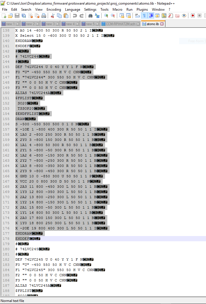
This is a component file. The section highlighted is a single component definition. The lines that start with X after it says DRAW are the pins. All that I do is create a list of pins with appropriate locations and insert them after any drawing entities, before the ENDDRAW line.
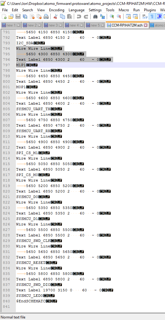
This is a KiCAD schematic file. It is a bit more free-form than the component file. If you look through it, it has component placement and definitions for wires and text labels for Nets, among other things. The easiest way to update this file with wires and nets is to delete the existing ones from within the schematic view in KiCAD (if any), save, and then open it in a text editor. If you scroll to the end of the file, you will find the EndSCHEMATC line. Insert your new stuff just above that line. Be careful to not break up multi-line items, otherwise it will cause an error and nothing will load after the error point in a file. I've highlighted a wire plus net text label for your reference. That is pretty much it. You could update the spreadsheet to match the exact coordinates on the spreadsheet, but I find it easy enough to move it once it is in, and you should give it a once-over anyhow.
You might wonder if it is worth the trouble. I found with systems that have common design features or just very complex ones with high pin counts along with multiplexed features on pins, something like this is really needed to keep track and not have small errors that are very hard to spot in complex designs.
The next step is to finish the schematic in KiCAD, iterate the pin and net configuration, and then move it into the PCB Layout.
Discussions
Become a Hackaday.io Member
Create an account to leave a comment. Already have an account? Log In.