 Guido - IW5ALZ


OVERVIEW: one small station, many listeners
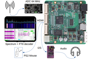
two-board setup
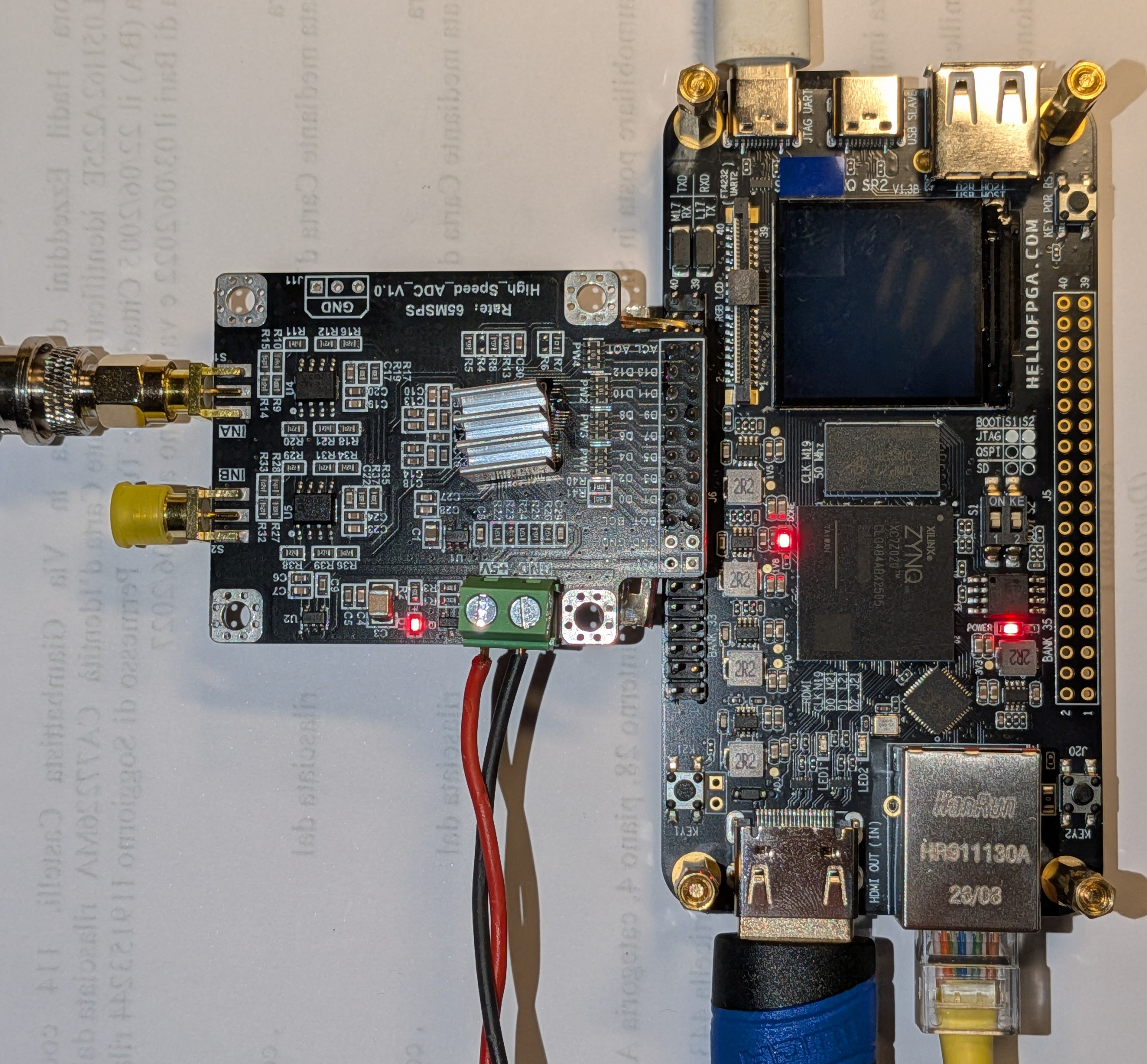
The AD9248 board (on the left) is the acquisition end:
- antenna input conditioning
- and high-speed conversion.
https://www.analog.com/media/en/technical-documentation/data-sheets/ad9248.pdf
The SmartZynq SP2 (on the right) is the processing end:
- it receives the sample stream,
- runs the digital signal processing pipeline in programmable logic,
- provides the operating system and network interface.
http://www.hellofpga.com/index.php/2024/01/21/smart-zynq-sp2/
The firmware turns a single digitized RF high speed stream into a set of configurable receive channels.
Each channel has its own digital oscillator, filter, decimator, and output stream.
This makes the hardware reusable: choose the frequencies in configuration instead of rewiring a receiver.
The intended first-use flow is:
1. Flash the supplied SD-card image or firmware bundle.
2. Connect the ADC board to the SmartZynq SP2 and attach the antenna.
3. Connect power and Ethernet.
4. Select a preset—such as multi-band FT8, WSPR monitoring, or a custom channel plan.
Channels are software, not hardware
The FPGA performs the repetitive high-rate work close to the ADC: digital down-conversion, filtering, decimation and demodulation. The processor side packages lower-rate IQ or audio streams for a local decoder, a network client, or logging software.
Example channel plans:
| Preset | Example allocation |
| FT8 watcher | One receive slice per selected amateur band |
| WSPR beacon monitor | Persistent WSPR slices plus spare experimental channels |
| Mixed digital bench | FT8, WSPR, CW/skimmer, and a general-purpose IQ stream |
Actual simultaneous channel count, usable coverage, and dynamic range will be documented from measured firmware builds.
Input filtering and antenna protection remain important, especially with strong nearby transmitters.
Why these two boards?
The AD9248 provides fast dual-channel conversion, while the SmartZynq SP2 pairs FPGA fabric—ideal for many parallel DDCs—with an embedded processor that can boot, configure the receiver, and serve results over Ethernet. Together they move the difficult hardware work into a repeatable two-board assembly and leave experimentation to firmware.
Block diagram
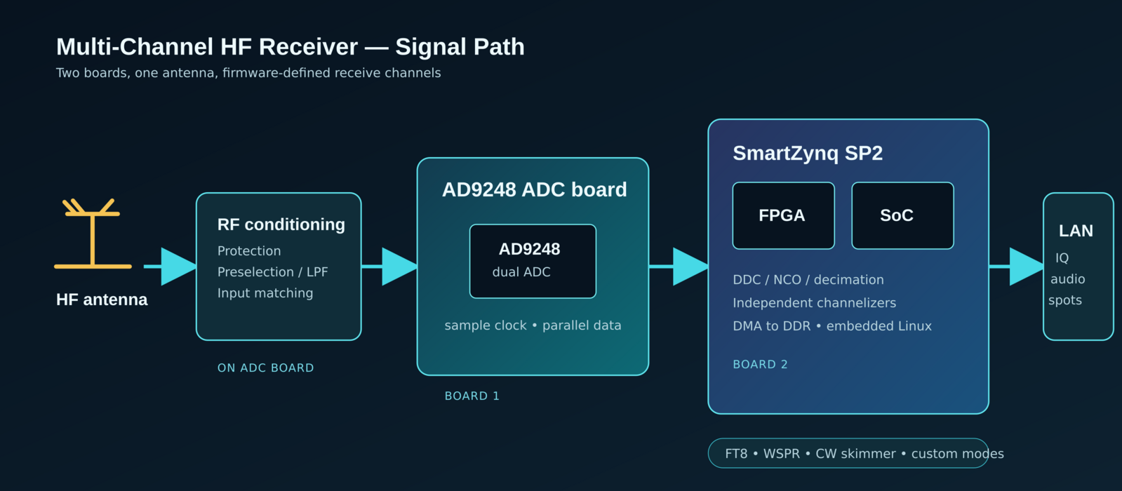
The antenna enters the ADC board, where it is protected, filtered, and matched before conversion.
Sample data crosses to the SmartZynq SP2, whose FPGA creates independent digital channels.
The SoC then exposes those channels as IQ, audio, or decoded/spot data over the network.
Project status (see the logs for details)
- The vendor Xillinux design rebuilt in Vivado 2026.1
- A 64 MS/s virtual RF source through the FPGA DDC
- USB/LSB audio generated in PL and played on an Ubuntu PC
- PS-programmable 79-symbol FT8 test waveform
- Why the AD9248 output needed offset-binary conversion
- From one verified receiver channel to eight planned channels
- Architecture and project presentation are in place.
Next milestones:
- test multi channel
- run some FT8 decoders on PS
The ADC, DDC and demod interface
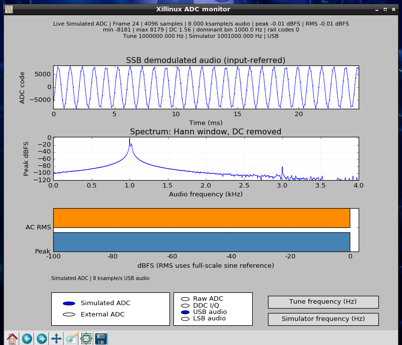
Using this interface you can set:
- source: an internal FT8 generator or the external Antenna
- data processing: raw ADC or DDC I/Q or demodulated SSB (USB or LSB)
- real time view and spectrum view
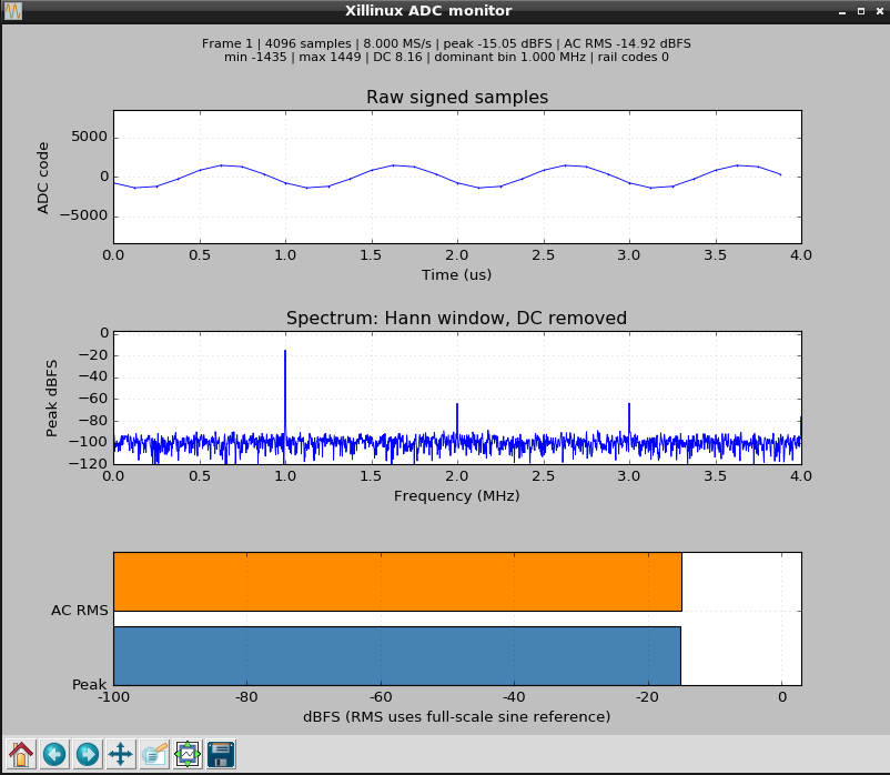
Receiving an external signal (1KHz USB)
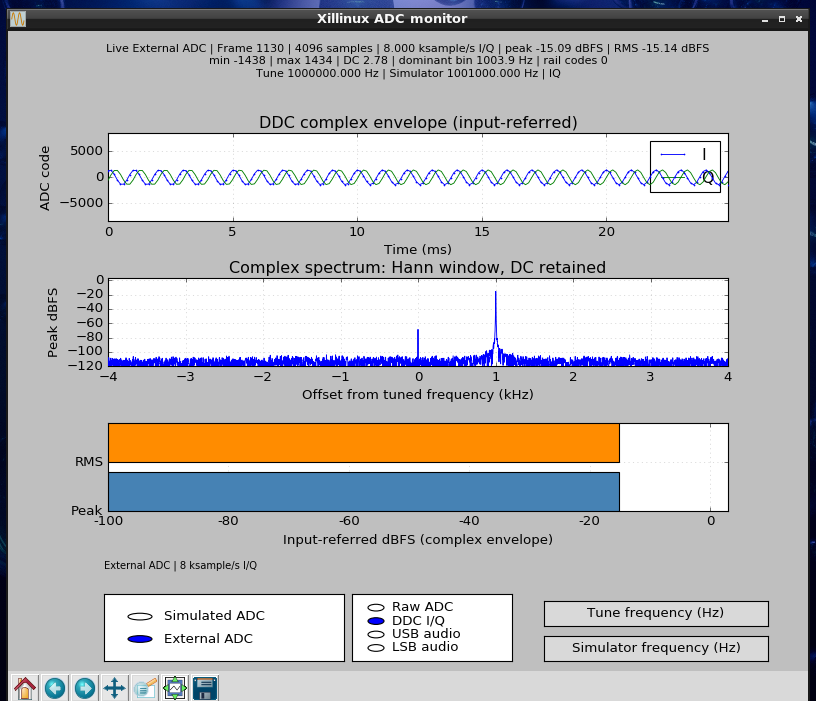
ADC - DDC - CIC FIR filtering - SSB demodulator Vivado Block design
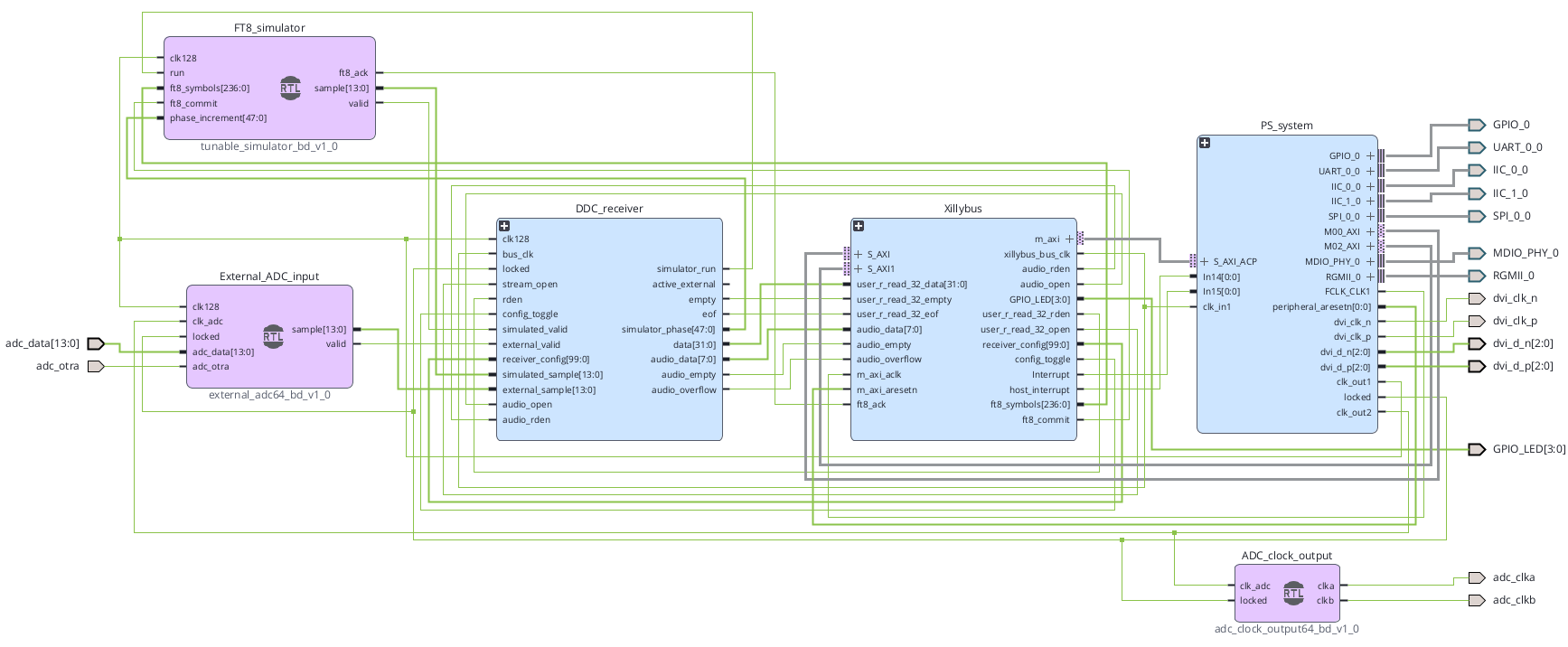
This is the top-level Vivado block design. It connects the Zynq processing system, the external ADC, the virtual FT8 source, the FPGA receiver chain, and the Xillybus DMA interfaces.
PS System is the vendor SmartZynq platform: the Zynq PS, DDR and AXI infrastructure, XillyVGA/HDMI output, Ethernet/RGMII, UART, GPIO, and clock/reset generation. It runs Xillinux and provides the AXI connections used by the FPGA logic.
External ADC Input receives the parallel AD9248 channel-A data and over-range signal. It runs in the ADC clock domain,...
Read more »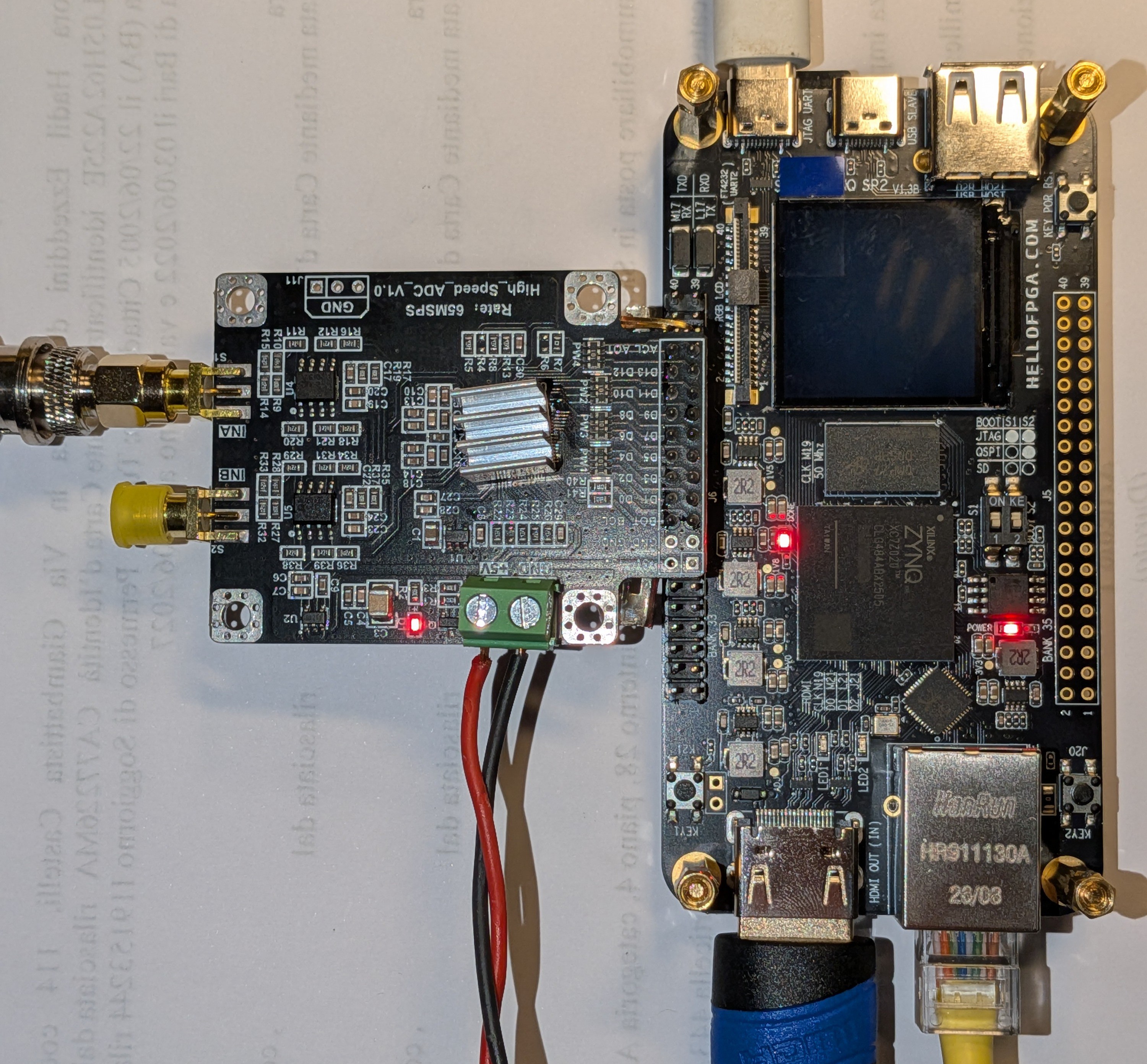

 Fabien-Chouteau
 Alberto Garlassi

 Mark Omo