 Marcel van Kervinck
[ Edit: I eventually settled for a totally different ALU design than sketched here! Ik keep this log entry just to preserve history. -MvK ]
We will do a custom ALU, not because we don't have any 74'181 IC's available, but because it is more fun.
There is a beautiful 12 chip MUX-based design out there, nicely described by Dieter Mueller. It even has a shift-right instruction which the 74181 is lacking. Without that it would be 10 chips. I'm tempted to use this design but I still worry about the many control lines that go in, 9 if I count correctly. Well, 8 if we drop de SHR support. Many control lines means many chips in the decoder, unless we use a ROM but that is slow.
That's why I consider something else, based on 6 chips per nibble, with less flexibility but therefore also fewer control lines. The necessary operations are there (A+B, A-B, A&B, A|B, A^B). There is also a "B" operation that we can use to load data without modifying it. We need that because all traffic to registers goes through the ALU in our design. In our data path we can also put AC on the BUS, so we have things like A+A. And there is an "A+1" that we will make use of in the STIX instruction ("store-and-increment-X") later on.
The main part is straightforward: three stages, some logic on top, some multiplexers in the middle to select intermediates and a final addition stage. With 4 control lines we can generate our desired functions plus a handful more that are not very useful, such as "(A ^ B) + 1". Of our functions, only "A|B" is a bit difficult to visualise, because there is no OR-chip in the circuit. It uses the identity A|B = (A&B)+(A^B) instead. Finally, we won't store the carry as we don't want to have a status register. Maybe in a later phase we can use the carry in some useful way.
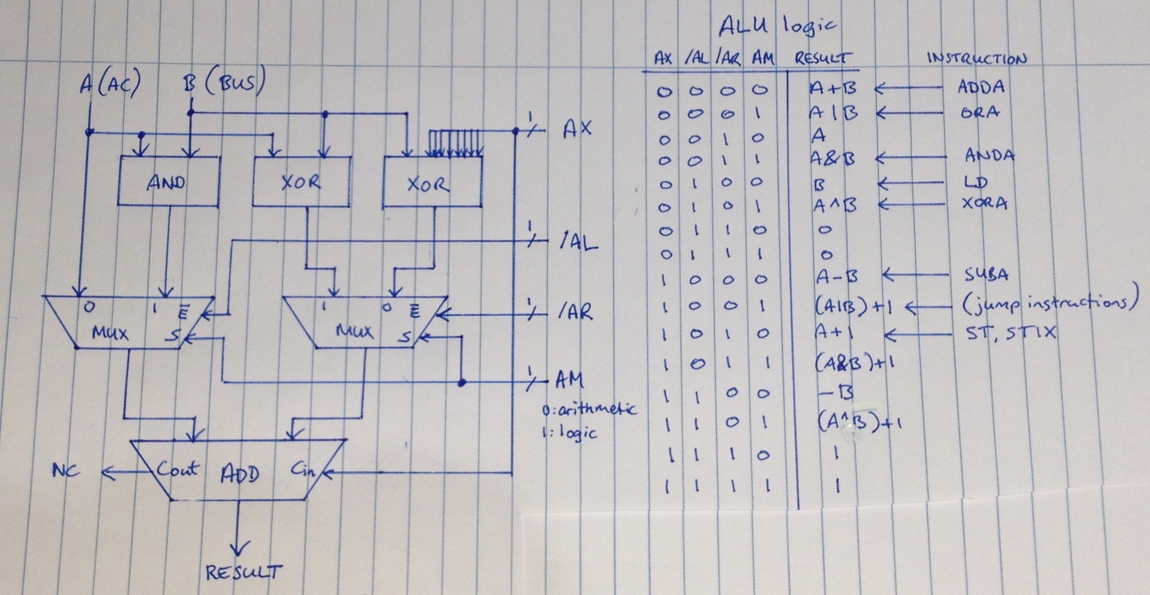
Four control lines is OK already. With that we could make an opcode scheme where 4 bits select the desired ALU operation immediately, without any further decoding, and let the other bits select the addressing modes. Then we assign the less useful codes to instructions that don't use the ALU, such as store and jump instructions. We need to derive the "write" and "jump" detectors with some logic but that shouldn't be hard. Also, during the first phase of the clock the "load" lines into the registers and the "write" line into the RAM must be muted anyway (for different reasons), which means there should be no worry for glitches while deriving these signals with combinatorial logic.
Still haven't decided yet on this one.
Discussions
Become a Hackaday.io Member
Create an account to leave a comment. Already have an account? Log In.
This project has 5 chips per nibble and '181 equivalence, or 10 chips for byte operations.
Are you sure? yes | no
Hi Marcel,
Take a look at my ALU design (https://hackaday.io/project/21193-aluminimum):
8x 8:1 MUXes + 1x quad XOR = 9 chips / nibble, with 3-bit CLA (fast!), 6 opcode bits (I is the logic operation or 0110 for arithmetic, M is logic/arithmetic mode selection, and SR is for right shift operation), but this can certainly be optimized further if not all 16 logic operations are required.
No explanation yet, I am still in the process of explaining computer history ;-)
But you can probably understand the Logisim file that provides the step-by-step optimizations that lead to this schematic.
Are you sure? yes | no
Nice !
Are you sure? yes | no
It is hard for me to judge. It looks quite interesting. In my project, 8 MUX chips and 2 adders take over the functionality of TWO 74'181s. So I have 5 chips for one 4-bit ALU. But I don't have shift-right. With 74LS, that would cost 1 more IC, so 6 per nibble.
Are you sure? yes | no