 Marcel van Kervinck
The control unit (CU) is the last thing to be worked out before committing to a build. The concept I had in mind requires 6 chips and I was slightly unhappy about that. After some thinking I came up with an idea that drops one chip from this unit. However, it requires that at some point I invert the clock signal using an XOR gate, whereas in my original plan this would be done with a NAND. Inverting the clock with a NAND worked fine in my previous VGA project. But the XOR is slightly slower, especially if used as an inverter, so it increases the phase shift a bit further. This inversion is on the critical path towards the RAM write-enable pin. A write into RAM is only allowed to happen in the second phase of the clock. In the first phase we have to stabilise the RAM address. We don't want any glitches there so we must be really sure this is going to fly.
That's why I built a small CU-RAM simulator and fed it fake instructions: read, read, write, write, read, read, write, write, etc.. so all possible execution orders are exercised. Then just measure what the resulting write-enable signal looks like. Here is the idea in a drawing:
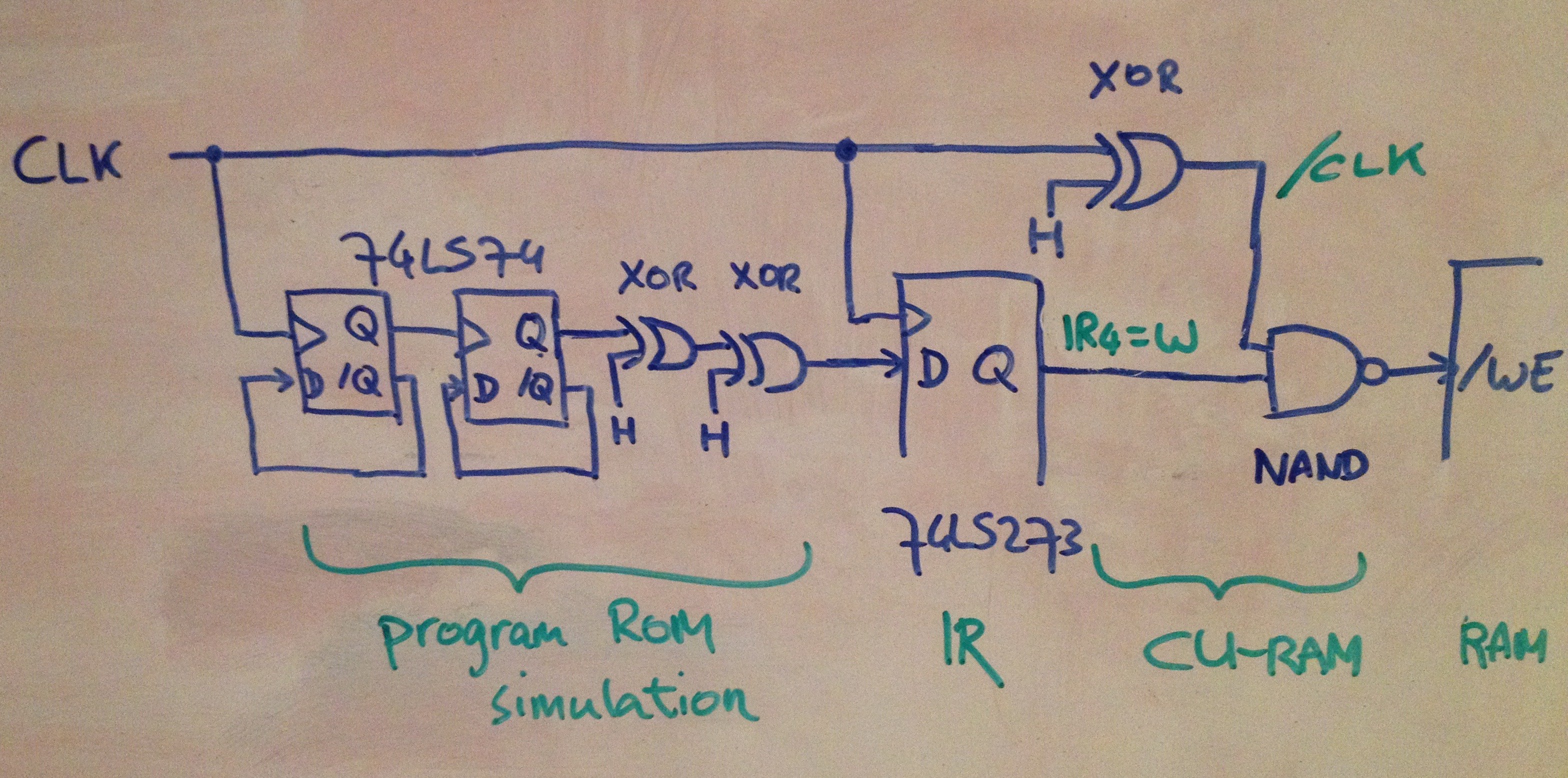
The fake instructions come from a 74LS74 dual-flipflop that just divides the clock by 4. This feeds into a 74LS273 that acts as IR register. (For fun, before entering IR, the signal goes through 2 bonus XOR inversions and picks up some delay there. This is not important but the gates were there anyway...) From the IR register it goes to the "real" NAND that on the other pin receives the XOR-inverted clock, just as in my intended design. Here the circuit on a breadboard:
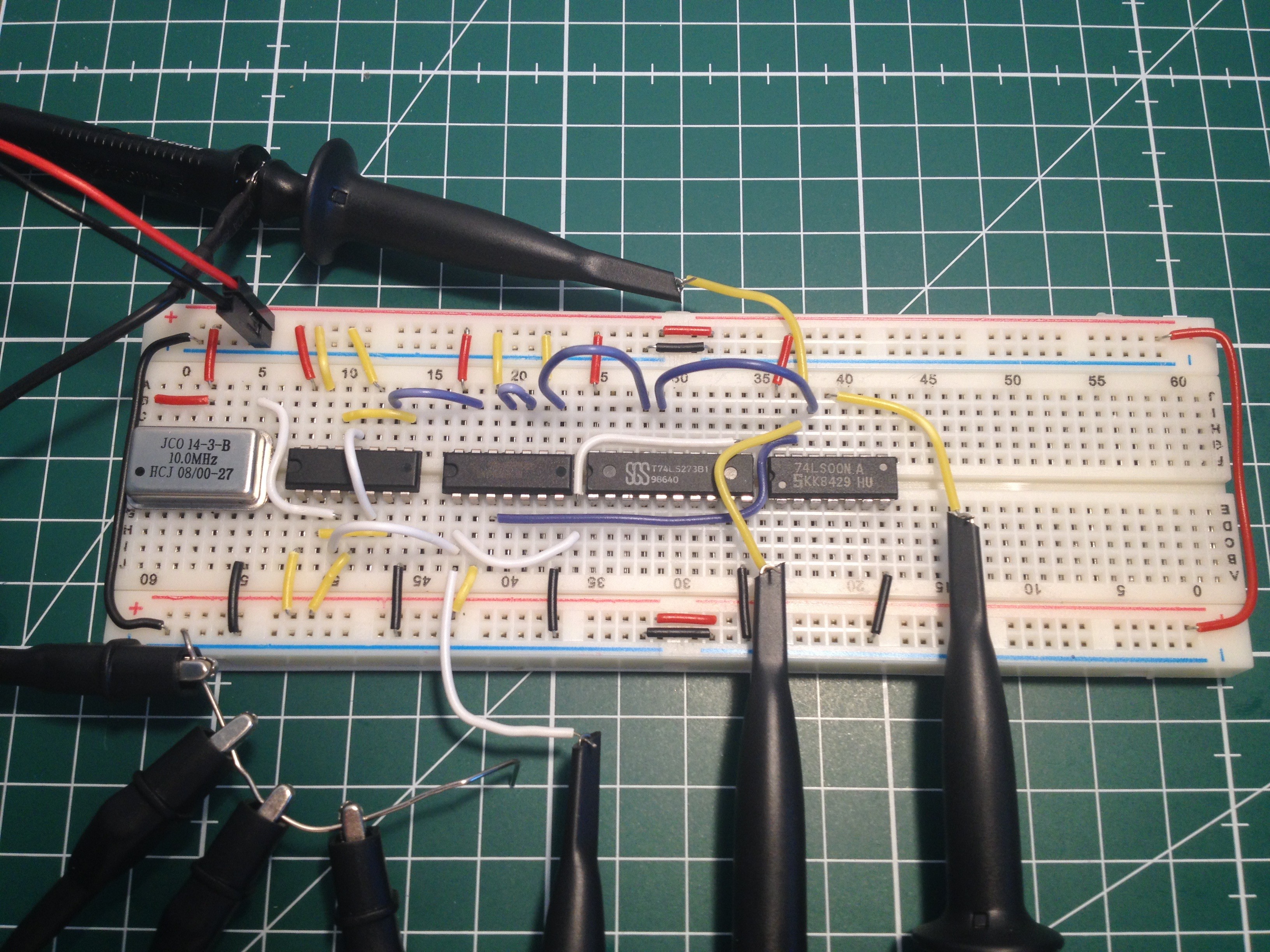
From left to right: 10 MHz clock, 74LS74 dual flip-flop, 74LS86 quad xor, 74LS273 register and a 74LS00 quad nand. Plus some probes. This is what we get:
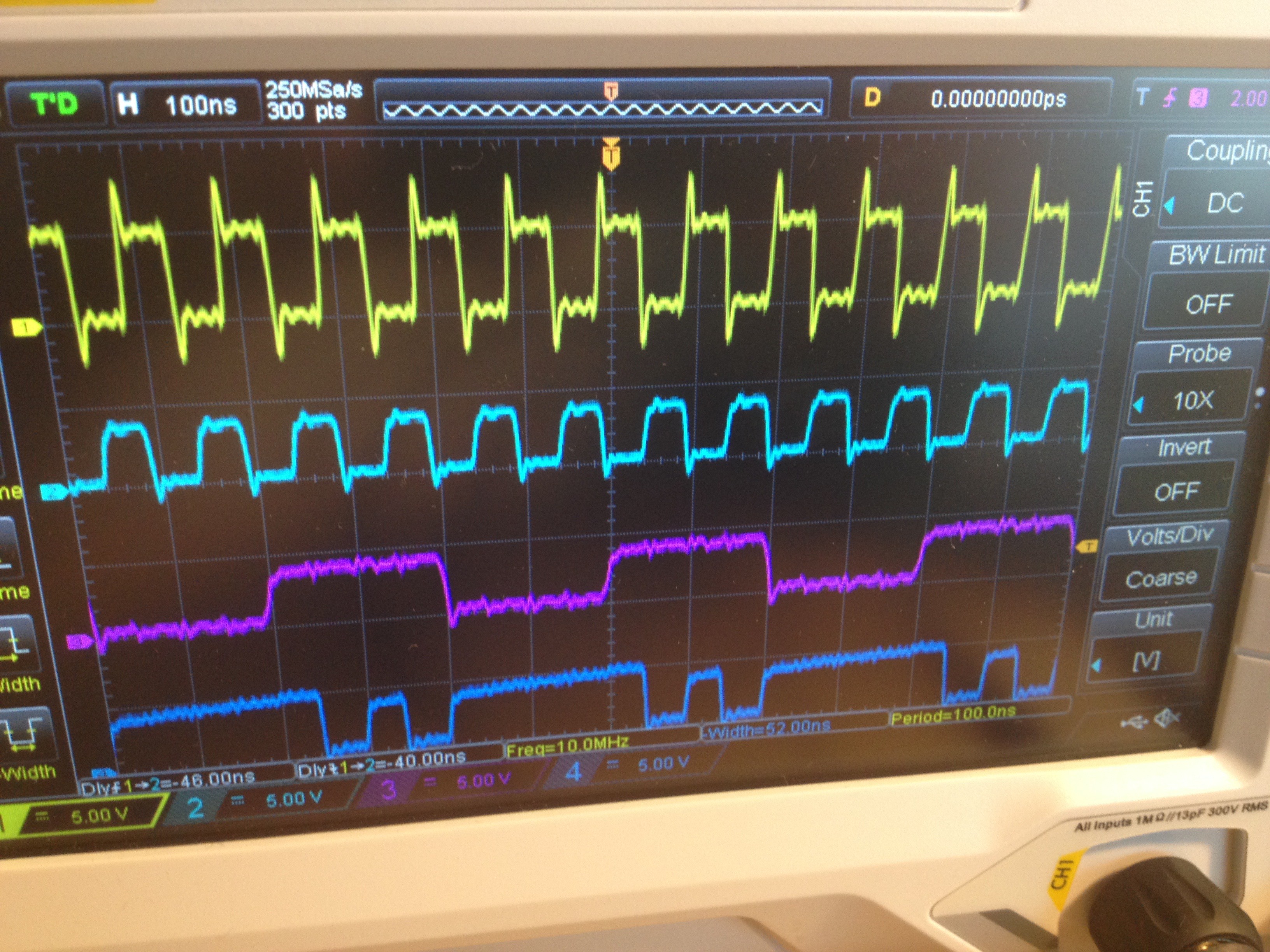
From top to bottom: yellow = clock, cyan = inverted clock with clearly some phase shift, purple = simulated instructions (low is read, high is write), and blue = the resulting write-enable signal that must go into RAM.
It works! We see nice pairs of negative write pulses and no glitches. Even better, with a 10 MHz clock the write pulse is still over 50 ns wide. For the 70 ns RAM I intend to use the write pulse has to be at least 50 ns. I wonder if the rest of the system can keep up with that as well.
Discussions
Become a Hackaday.io Member
Create an account to leave a comment. Already have an account? Log In.