Marcel van Kervinck
-
Ground control
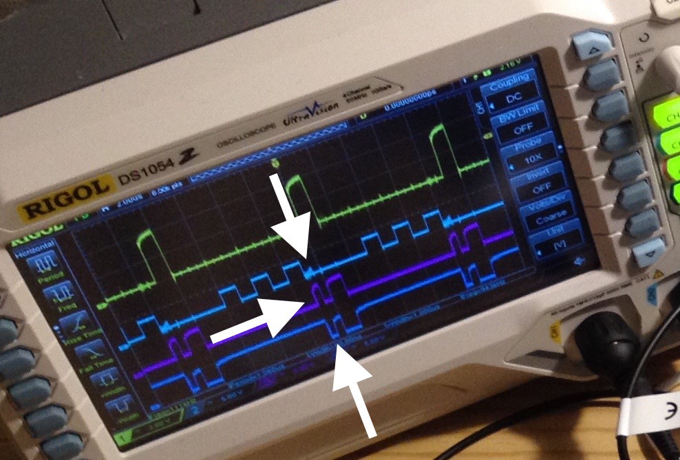
05/02/2017 at 11:15 • 2 commentsThis is the glitch I was still contemplating yesterday:
![]()
It isn't a EEPROM timing issue after all. Low signals into the instruction decoder just weren't always low enough. The culprit turned out to be the IR register's ground pin:
![]()
Signals look much better with that sorted out:
![]()
Next is the verification of the ALU.
-
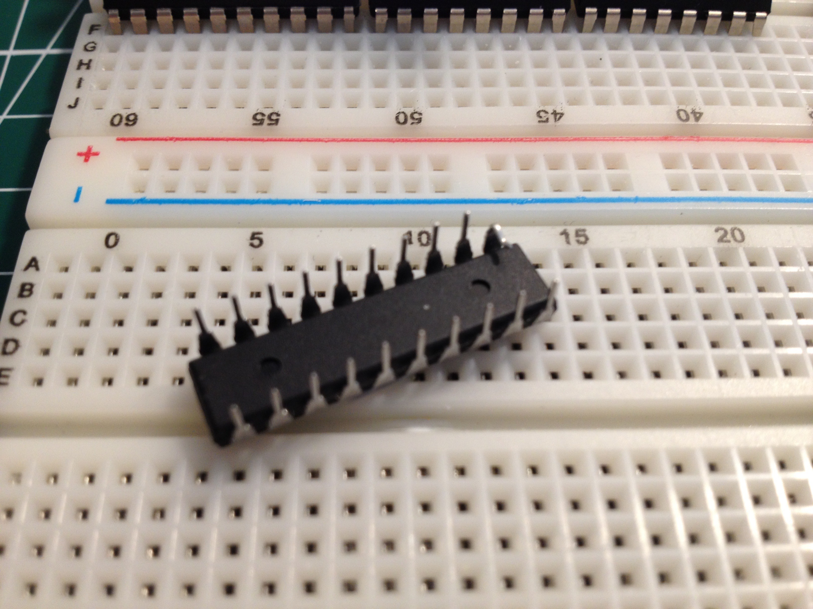
74LS377 for speed
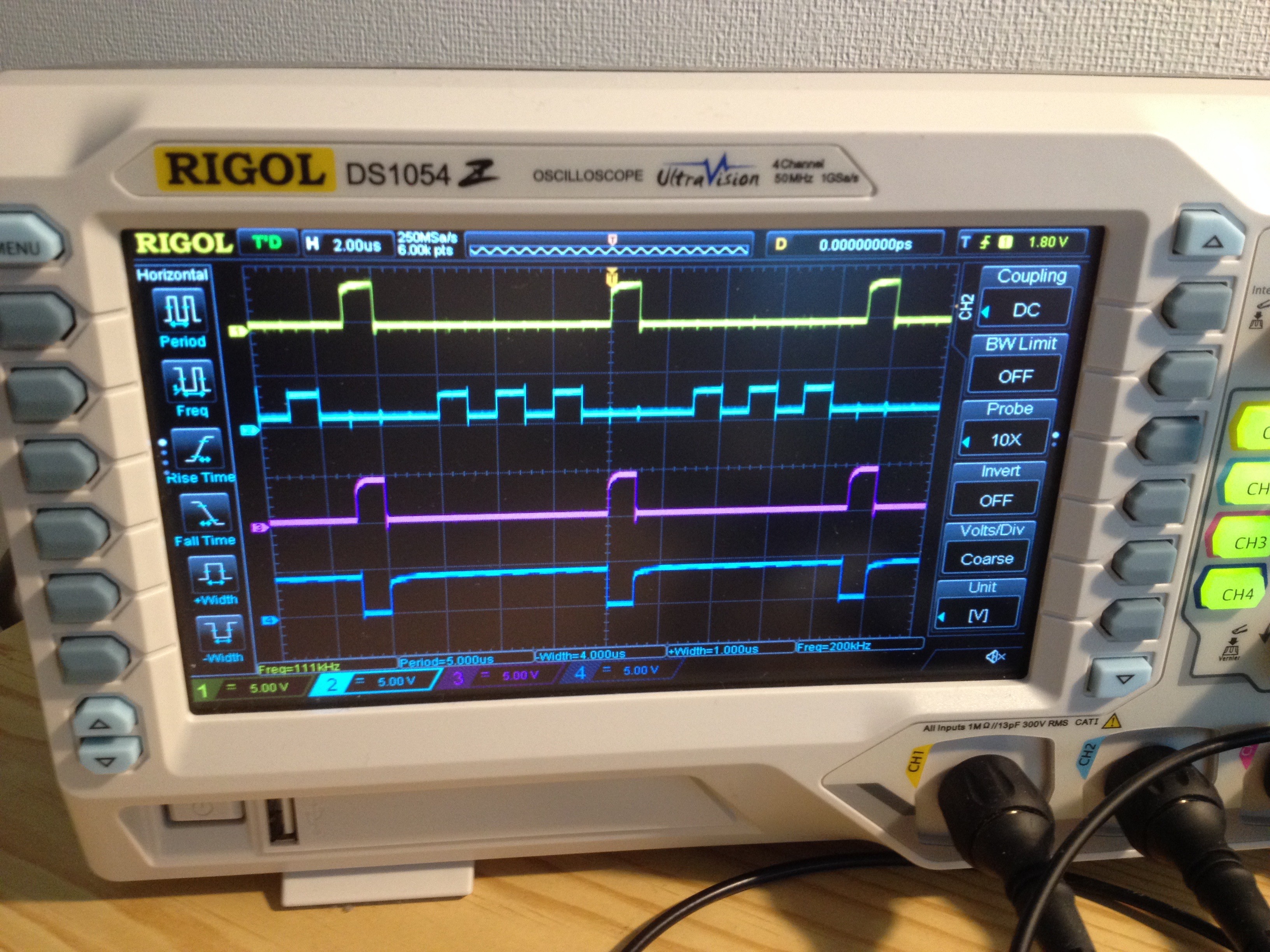
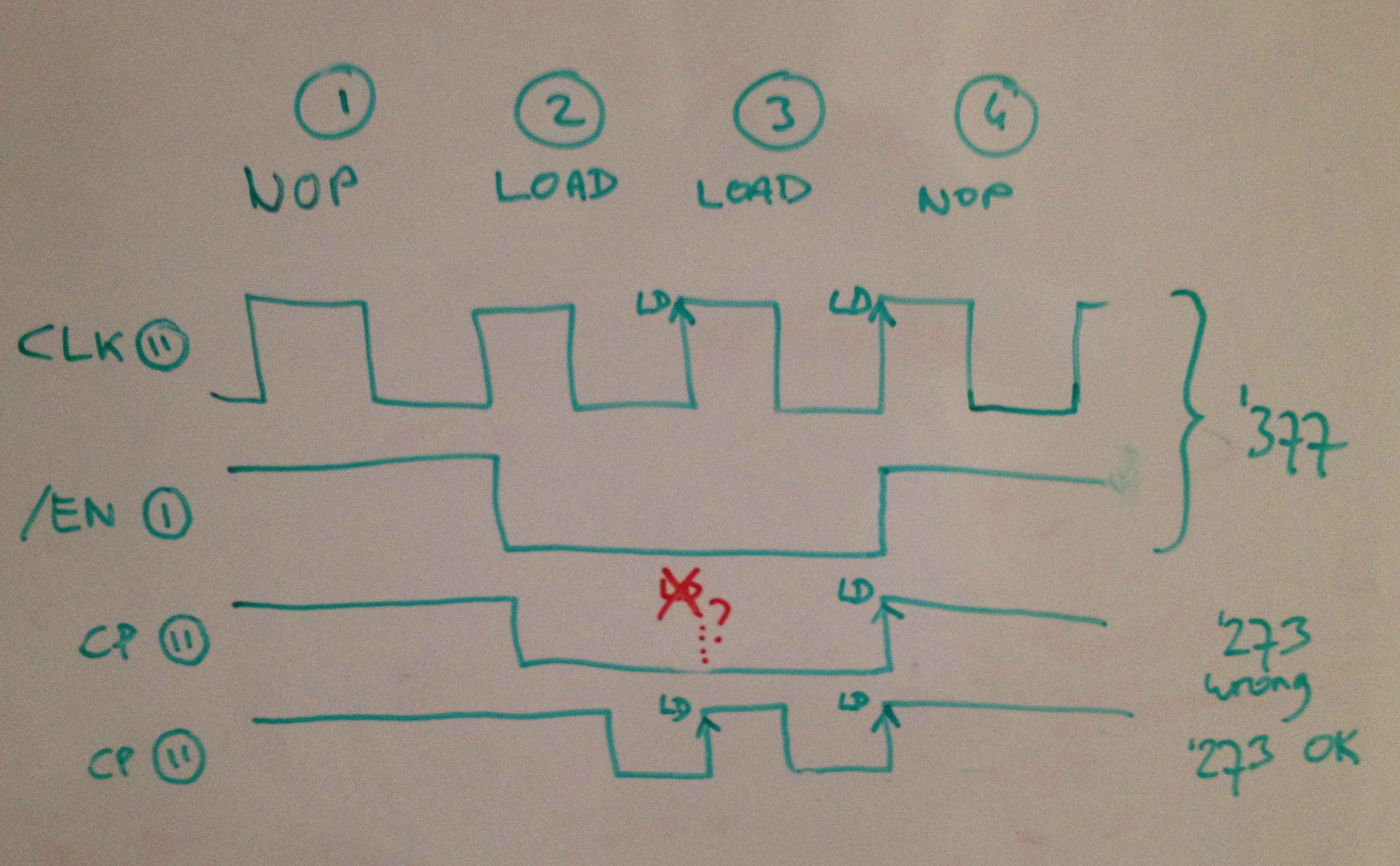
05/06/2017 at 13:34 • 5 commentsThe project uses '377 chips for the accumulator and output registers instead of the more obvious '273. The difference is pin 1. In the '273 this is a reset pin and we don't need that. In the '377 this is a (negative) enable pin, and that is very useful. It simplifies the control logic in the case of consecutive loads. To see why, consider the timing diagram:
![]()
The '377 can be wired directly to the clock on pin 11 and to the register address decoder on pin 1. If we were to use the '273, we only have pin 11. But if that is connected to the decoder, as in the middle case, consecutive loads don't work: only the last load will give a positive edge and therefore transfer a value. The earlier load values are missed. This is not good for the accumulator and for output, as each value can be important.
To make the '273 work, you need to put the logical OR of CLK and /EN on pin 11, so you get two edges. But the control logic doesn't have spare OR gates available, so that would cost an additional 74LS32 chip. Either that, or it would cost speed, because you can simulate the effect in software with NOP instructions. But then we are also stuck with half the horizontal resolution for the video signal. Not nice.
For the other registers these considerations don't hold and they can keep using the '273.
Today my order of '377 IC's has arrived, so the project can continue.
![]()
-
Fibonacci
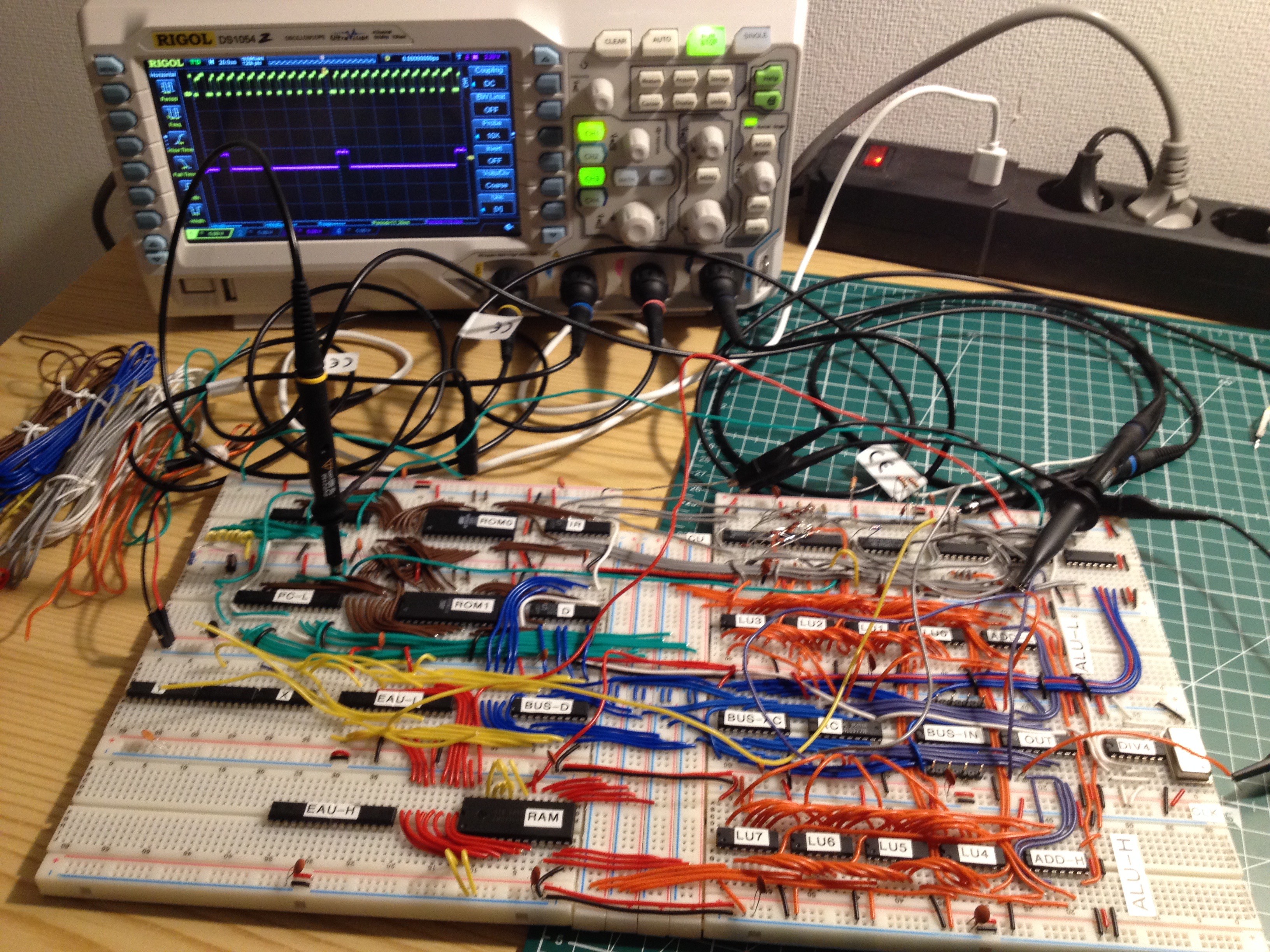
05/11/2017 at 00:33 • 2 commentsWith the ALU verified and the RAM connected, today the breadboard determined that the first 8-bit Fibonacci number is 144.
0000 0000  ld   $00    ; outer loop
0001 c200  st   [$00]  ; a=0
0002 0001  ld   $01    ; b=1
0003 fc0a  bra  $0a
0004 0200  nop         ; (pipelining)
0005 0100  ld   [$00]  ; inner loop
0006 c202  st   [$02]  ; tmp=a
0007 0101  ld   [$01]
0008 c200  st   [$00]  ; a=b
0009 8102  adda [$02]
000a c201  st   [$01]  ; b+=tmp
000b 1a00  ld   ac,out ; emit next Fibonacci number
000c f405  bge  $05    ; repeat if bit7 is still 0
000d 0200  nop         ; (pipelining)
000e fc00  bra  $00    ; start over again
000f 0200  nop         ; (pipelining)
The inner loop runs 12 times (1, 1, 2, 3, 5, .... 89, 144). The entire thing takes 110 cycles. Both are exactly as expected. It can be done faster but I didn't optimise the assembly to maintain my sanity.
I also hooked up a cute little MCP100-475 to the program counter reset line. This gives a controlled reset during power up. The circuit is now 90% wired. Only the high memory address control and some diodes are missing for full functionality.
![]()
-
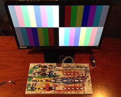
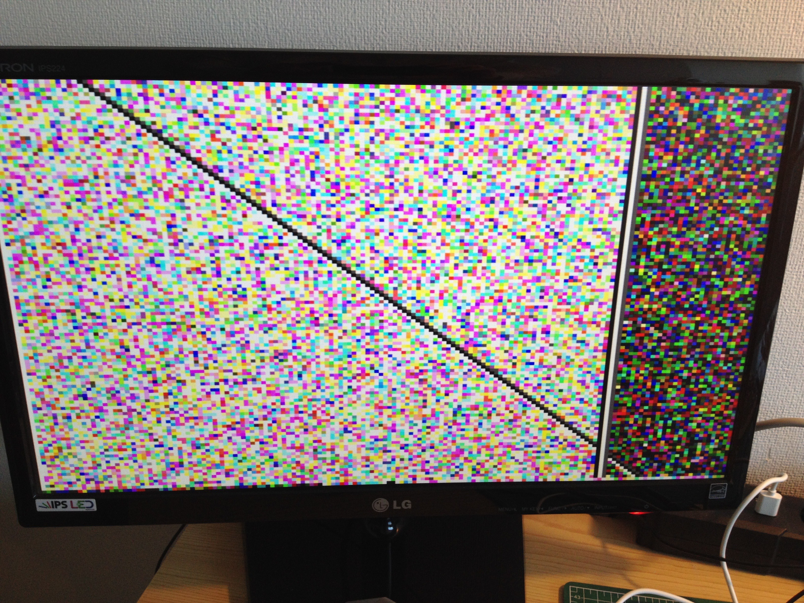
First video out
05/13/2017 at 18:23 • 0 commentsIt seems I have reached the base camp. The el-cheapo 7-inch LCD monitor on the right is connected to the output port of my breadboard TTL computer. The computer is now running at 6.3MHz and runs a software loop that generates a VGA test signal. The colors look a bit off, and still not all wiring is done and tidied up, but the mountain top is definitely in sight.
![]()
As far as I can check with the oscilloscope, the signals are behaving nicely according to the VGA industry standard 640x480 at 60Hz. Yellow is the vertical sync and light blue is the horizontal sync.
![]()
The disassembly of the code:
0000 0009  ld   $09 ; setup for 10 lines vertical front porch
0001 a001  suba $01 ; next line in vertical blank
0002 c200  st   [$00]
0003 0200  nop
0004 0008  ld   $08 ; entry point for starting a new frame, inside the first hsync
0005 ec05  bne  $05
0006 a001  suba $01
0007 0200  nop
0008 18c0  ld   $c0,out ; end of first hsync in frame
0009 0055  ld   $55
000a ec0a  bne  $0a
000b a001  suba $01
000c 0100  ld   [$00]
000d ec01  bne  $01
000e 1880  ld   $80,out ; new hsync start
000f 000a  ld   $0a
0010 ec10  bne  $10
0011 a001  suba $01
0012 18c0  ld   $c0,out ; hsync end
0013 0054  ld   $54
0014 ec14  bne  $14
0015 a001  suba $01
0016 1840  ld   $40,out ; vsync start
0017 0200  nop
0018 0200  nop
0019 0200  nop
001a 1800  ld   $00,out ; hsync during vsync
001b 000a  ld   $0a
001c ec1c  bne  $1c
001d a001  suba $01
001e 1840  ld   $40,out ; hsync end
001f 0056  ld   $56
0020 ec20  bne  $20
0021 a001  suba $01
0022 1800  ld   $00,out ; hsync during vsync
0023 000a  ld   $0a
0024 ec24  bne  $24
0025 a001  suba $01
0026 1840  ld   $40,out ; back porch
0027 0054  ld   $54
0028 ec28  bne  $28
0029 a001  suba $01
002a 18c0  ld   $c0,out ; 33 lines black
002b 0200  nop
002c 0200  nop
002d 0020  ld   $20
002e 1880  ld   $80,out
002f a001  suba $01
0030 c200  st   [$00]
0031 0009  ld   $09
0032 ec32  bne  $32
0033 a001  suba $01
0034 18c0  ld   $c0,out
0035 0055  ld   $55
0036 ec36  bne  $36
0037 a001  suba $01
0038 0100  ld   [$00]
0039 ec2f  bne  $2f
003a 1880  ld   $80,out
003b 000a  ld   $0a
003c ec3c  bne  $3c
003d a001  suba $01
003e 18c0  ld   $c0,out
003f 0055  ld   $55
0040 ec40  bne  $40
0041 a001  suba $01
0042 0200  nop
0043 00e0  ld   $e0
0044 1880  ld   $80,out
0045 a001  suba $01
0046 c200  st   [$00]
0047 0009  ld   $09
0048 ec48  bne  $48
0049 a001  suba $01
004a 18c0  ld   $c0,out
004b 0004  ld   $04
004c ec4c  bne  $4c
004d a001  suba $01
004e 18d5  ld   $d5,out ; first colors
004f 0003  ld   $03     ; 9 clock delay
0050 ec50  bne  $50
0051 a001  suba $01
0052 18d7  ld   $d7,out ; second color bar
0053 0003  ld   $03
0054 ec54  bne  $54
0055 a001  suba $01
0056 18dd  ld   $dd,out ; third color bar
[...snip...]
008a 18ea  ld   $ea,out ; last color bar
008b 0003  ld   $03
008c ec8c  bne  $8c
008d a001  suba $01
008e 18c0  ld   $c0,out ; back to black (front porch)
008f 0200  nop
0090 0100  ld   [$00]
0091 ec45  bne  $45     ; repeat for 480-256 = 224 lines
0092 1880  ld   $80,out ; hsync start
0093 a001  suba $01
0094 c200  st   [$00]
0095 0009  ld   $09
0096 ec96  bne  $96
0097 a001  suba $01
0098 18c0  ld   $c0,out ; hsync end
0099 0004  ld   $04
009a ec9a  bne  $9a
009b a001  suba $01
009c 18ea  ld   $ea,out ; second half of screen (256 lines)
009d 0003  ld   $03
009e ec9e  bne  $9e
009f a001  suba $01
[...snip...]
00e1 0008  ld   $08
00e2 fc04  bra  $04 ; to new frame
00e3 c200  st   [$00]
-
Homebrew CPU webring
05/21/2017 at 08:40 • 0 commentsMy breadboard TTL color computer is now included in David R. Brooks' Homebrew CPU webring. How cool is that!
![]()
In the meantime I have figured out how to mix video with application code. Next week we'll have a 5-day holiday, and if there are some rainy days in there I expect to get some animated output from this thing by then.
-
Two birds with one stone
05/21/2017 at 16:01 • 2 commentsAn Atari joystick will do as input device for the games I have in mind. But the breadboard computer has the potential to run a BASIC. For that, keyboard input would be great. USB is out of the question, and even PS/2 looks a bit involved. A simple matrix keyboard would be a better starting point.
Also, at some point I'll need an enclosure to keep dust out and to be able to bring it to places.
Today, I might have stumbled upon the solution for both problems.
![]()
[ Edit: to the millions of voices that suddenly cried out in terror: it had a broken PLA chip ]
-
First pixels
05/25/2017 at 16:25 • 0 comments160x120 in 64 colors, simply displaying uninitialised SRAM. A bit unstable, but a nice little step. All wiring is now connected. The next steps are to get stable signals, tidy up the wiring and make more interesting software.
![]()
-
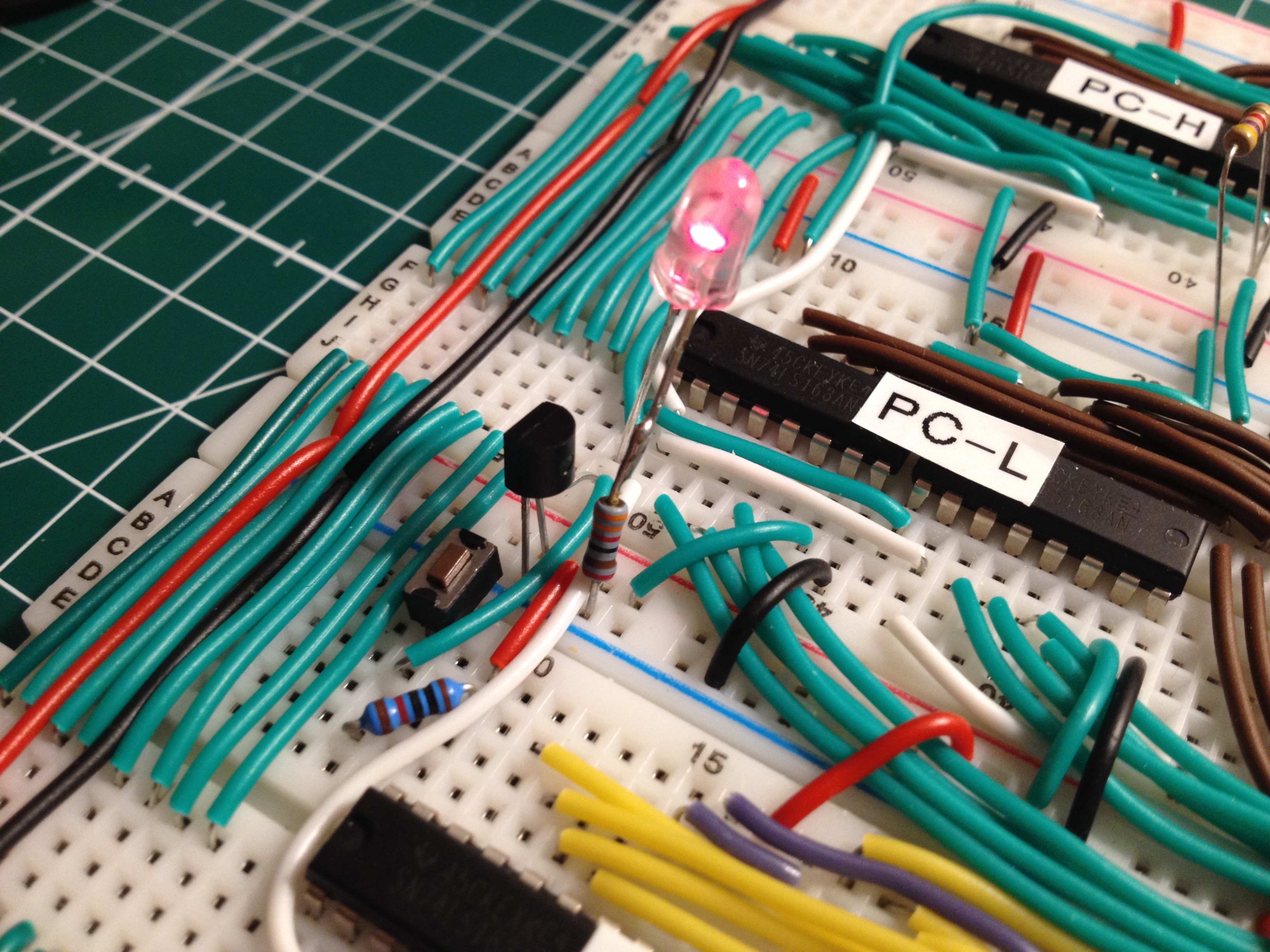
Stable video with help of a canary
05/27/2017 at 12:33 • 0 commentsThe control unit (CU) uses decoder IC's and diodes for decoding the operation and addressing modes. I'm toying with plain 1N4148 (silicon), 1N60 and BAT85 (both Schottky) diodes. Surprisingly, all seem to work pretty well. Here they are all mixed more or less randomly on the breadboard.
![]()
The diodes between INS (74LS155) and INV (74LS240) form the operation decoding ROM matrix. The diodes connected to MODE (75LS138) pull the control lines for register loads and RAM address generation. The diode mess looks fragile, but in reality it all stays in place rather well.
When combining diodes with TTL, there is only 400mV voltage drop to play with before entering undefined territory. Some of the diode logic outputs travel all the way across the circuit, which means that supply voltage and ground differences must be controlled over that distance. Also, 74LS requires 4.75V as absolute minimum, or no more than 5% drop.
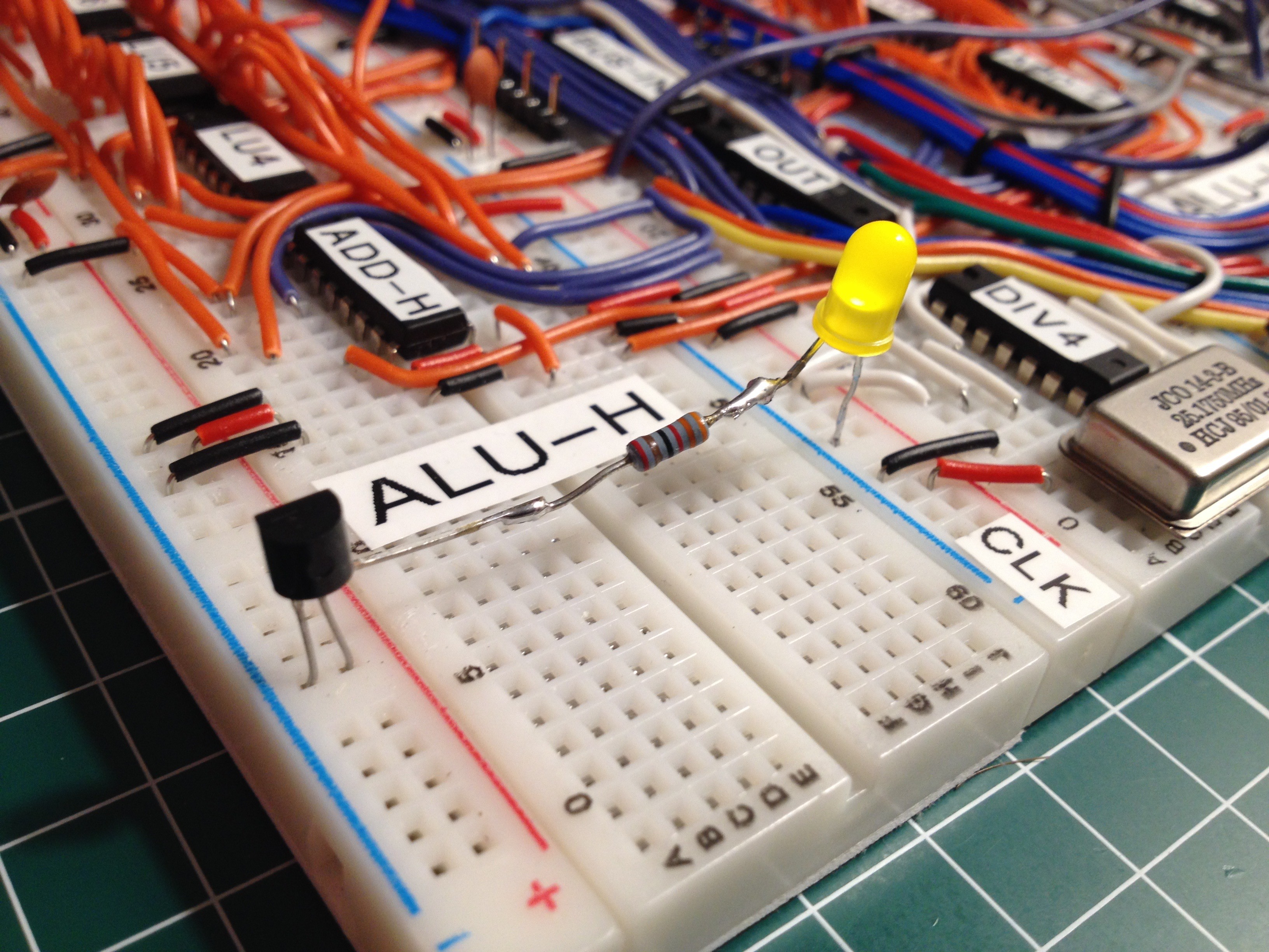
When I installed the supervisory MCP100 some weeks ago, I already noticed that I had to connect the 5V supply on the same segment in order to boot. If I connected it further away, it simply wouldn't release the reset. This means there is too much resistance between the segments, more than the equivalent of 250mV. A couple of extra bridges solves that. But to troubleshoot this, I found a useful second use for the MCP:
First recall that the MCP keeps the reset line low for as long as the supply voltage is not stable above 4.75V. (Well, the MCP100-475DI/TO does that. In ordering these, every letter means something important). In my circuit it sits next to the reset button, as you can see here:
![]()
You can spot the reset switch with its 10kΩ pull-up resistor. It controls pin 1, or /CLR, of the PC counter IC's (all four of them). The red LED is just lurking on the reset line as an indicator. The MCP is the three-legged black component that looks like a transistor. It has one leg on the reset line. The other two legs are on Vcc and GND. It is a clever and useful little device. Now it turns out you can make a super easy voltage tester from an MCP, an LED and a current limiting resistor (330Ω), as follows:
![]()
The "reset" leg is now connected to the LED and not to the circuit. If the LED is on, the voltage difference on the supply rails is stable above 4.75V. With this device it is easy to test the voltages everywhere, much easier than with a multimeter or scope. I call this the "canary" because of the yellow light, and because when the light goes out, it signals that that part of the circuit is in danger.
With all voltages controlled, the video image is now stable. I'm still emitting uninitialised SRAM data, but to verify that I'm streaming from the right addresses, I let the CPU draw some lines across the screen, vertically and diagonally. All addressing modes and registers are now exercised, so this is a pretty good system test.![]()
-
On the move
05/28/2017 at 14:06 • 0 commentsFirst moving video output from my breadboard TTL color computer. Again, the test image is just uninitialised SRAM garbage with some lines drawn over it. Line 60 to 90 are scrolling 1 pixel per frame.
The scrolling looks a bit jumpy in the recording, but that is just the mismatch between the camera and monitor frequencies. In real life it is stable and smooth.
-
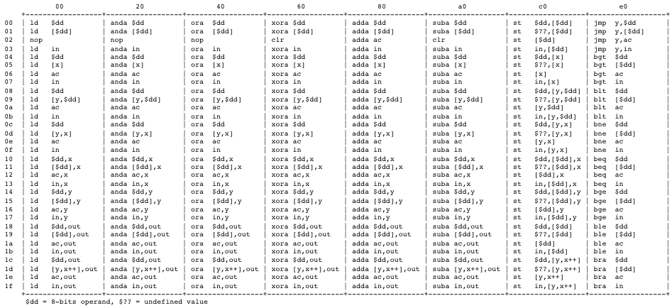
Undefined opcodes
05/29/2017 at 04:54 • 0 commentsFrom the assembler/disassembler it is easy to generate a complete instruction table. Most opcodes result in a valid instruction. Only memory writes while RAM is on the bus result in an undefined value ($??) being stored.
![]()
I found out I had some undefined instructions that are actually very useful. They store a value in memory as well as in X or Y. Their existence is entirely accidental: Unlike AC and OUT, the X and Y registers are not "muted" when we are writing to memory. The purpose of muting is solely to reuse all addressing modes in store instructions, but without destroying the contents of AC or OUT. As X and Y don't have addressing modes that AC and OUT already have as well, I didn't bother to give them an OR-gate that suppresses the enable signal to them ("you don't need these modes").
This omission turns out to be quite useful! Because X and Y are essentially "write-only" registers, each time you use them and you're not sure of their value you have to reload them. Now you can first do a computation, in AC, and then move the result both to X/Y and also back to memory. Both value transfers happen in the same clock cycle. With that, you can easily keep track of what is supposed to be in X/Y in the zero page. I suppose this will be used a lot. I already use it in the video loop.
Now they are no longer undefined. They are part of the family.
Gigatron TTL microcomputer
Just because! A home computer without microprocessor